

Plasma display device and drive method
A technology of display equipment and driving method, applied in static indicators, instruments, etc., can solve problems such as shutdown, crash, discharge unit rise, etc., and achieve great economic value and remarkable effect.
- Summary
- Abstract
- Description
- Claims
- Application Information
AI Technical Summary
Problems solved by technology
Method used
Image

Examples
Embodiment 1
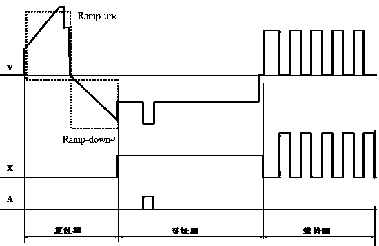
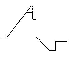
[0022] Design concept: On the basis of the original PDP Y electrode driving waveform, the highest voltage of the waveform Ramp-up phase of the first subfield reset period of the first frame is increased.
[0023] Basic principle: Increase the voltage of the Ramp-up stage, that is, further strengthen the weak dark discharge intensity of the discharge unit, and obtain more negative wall charge accumulation on the Y electrode (the A and X electrode dielectric layers accumulate positive charges), and at the same time Offset the continuous increase of external voltage and keep the discharge cell at the ignition voltage (the so-called ignition voltage is the minimum driving voltage for driving the discharge cell (3 discharge cells equals one pixel)) state, so that the subsequent discharge can be based on a consistent state get on.
[0024] figure 2 Shown are two-stage waveform diagrams of the driving waveforms Ramp-up and Ramp-down of the plasma display device according to the first emb...
Embodiment 2
[0027] Design concept: On the basis of the original PDP Y electrode driving waveform, the lowest voltage of the waveform Ramp-down during the reset period of the first subfield of the first frame is reduced.
[0028] Basic principle: Decrease the voltage of the Ramp-down stage, which actually increases the Ramp-down voltage, and the voltage direction is negative. Due to the accumulation of enough wall charges in the Ramp-up stage, the erasing discharge capacity is enhanced during the slow decline of Ramp-down. All discharge cells generate erasing discharge to erase the wall charges and enough generated in the Ramp-up stage. A large amount of space ions will form uniform residual wall charges that can stably generate address discharge, thereby reducing the ignition voltage of the discharge cell and eliminating the discharge delay.
[0029] The amount of voltage drop in the ramp-down stage varies according to the actual situation.
[0030] This embodiment can be used in combination wi...
Embodiment 3
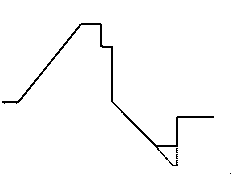
[0032] Design concept: A voltage is superimposed on the basis of the Ramp-down phase of the reset period of the first subfield of the first frame and the X_shelf reference voltage of the address period ( Figure 4 ).
[0033] Basic principle: On the basis of not changing the PDP Y electrode driving waveform, superimpose an X_shelf voltage on the original X_shelf voltage for the Ramp-down and address period to increase the discharge intensity between the Y electrode and the X electrode, and make the surface of the electrode dielectric layer Accumulate enough wall charges and generate enough space ions, so as to reduce the ignition voltage of the discharge unit to avoid discharge delay, and completely eliminate the low discharge failure after switching between black background pictures. Its purpose is to reduce the voltage of the discharge unit Vf and eliminate the discharge delay.
[0034] The voltage superimposed on the basis of the reference X_shelf voltage varies according to th...
PUM
 Abstract
Description
Claims
Application Information