IGBT device and forming method thereof

A device and semiconductor technology, applied in the field of IGBT devices and their formation, can solve problems such as poor performance of IGBT devices, and achieve the effect of improving yield

Active Publication Date: 2014-06-11
INST OF MICROELECTRONICS CHINESE ACAD OF SCI +2
View PDF5 Cites 5 Cited by
  • Summary
  • Abstract
  • Description
  • Claims
  • Application Information

AI Technical Summary

Problems solved by technology

However, the performance of IGBT devices in the prior art is not good

Method used


Image

  • IGBT device and forming method thereof
  • IGBT device and forming method thereof
  • IGBT device and forming method thereof

Examples


Embodiment 1

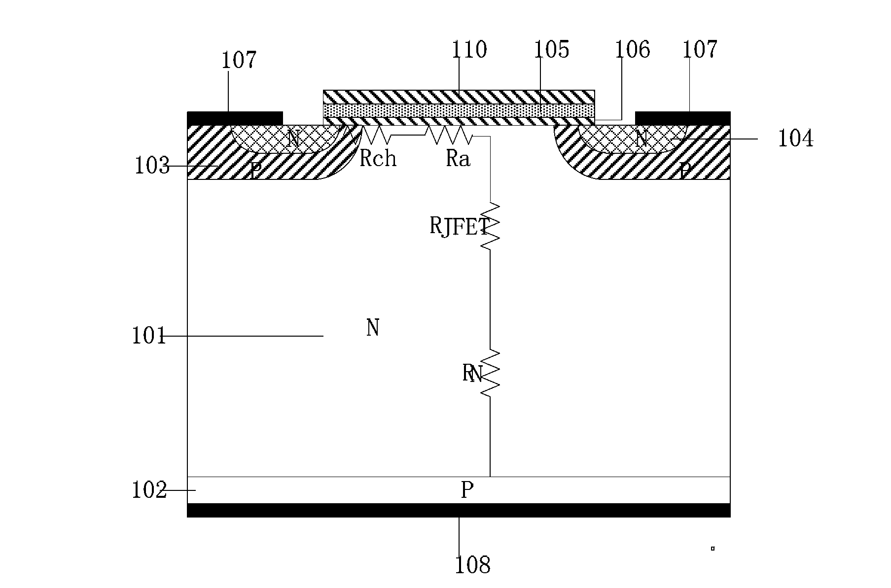
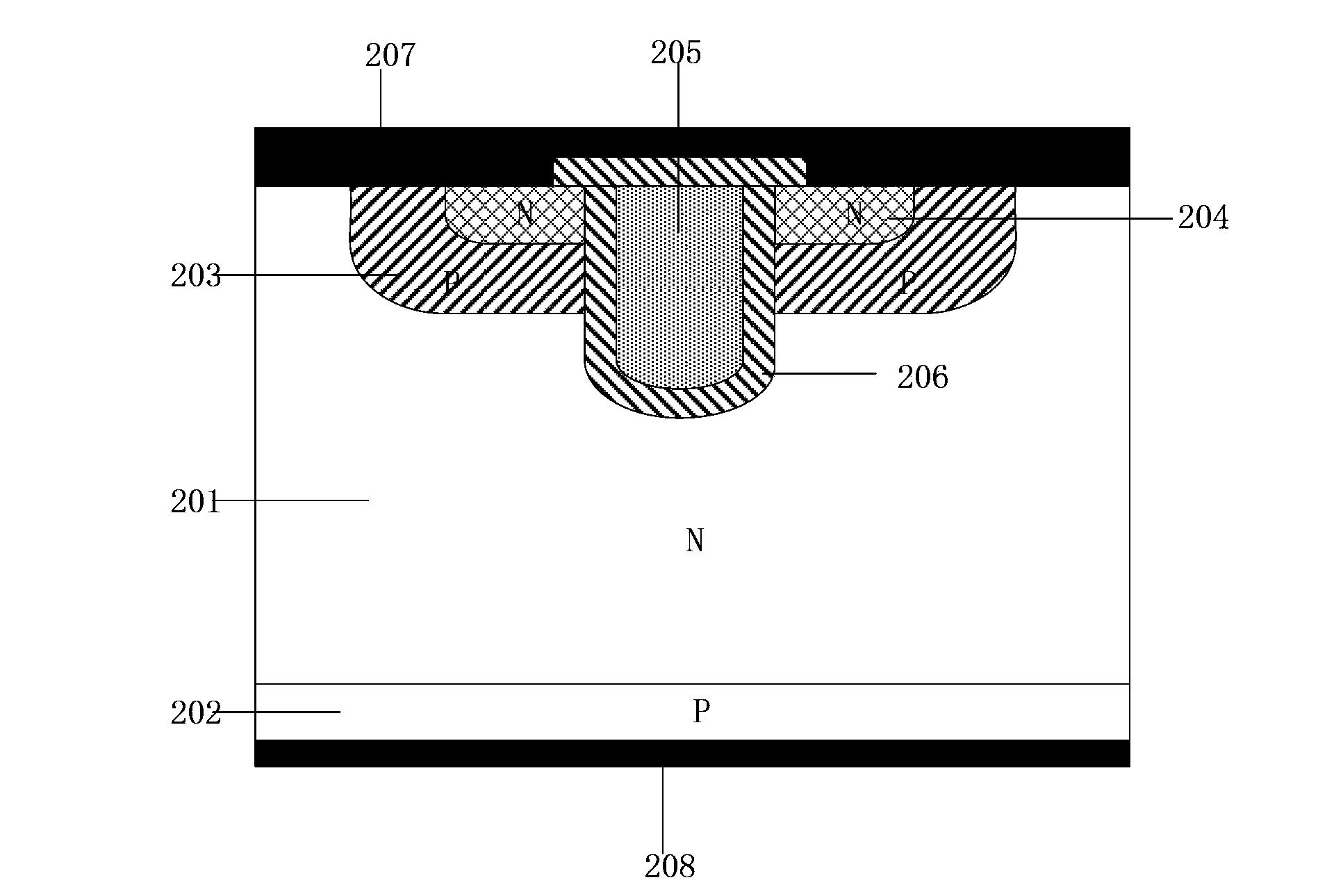
[0068] Such as Figure 5 As shown, the IGBT device provided by the embodiment of the present invention includes:

[0069] A semiconductor substrate including a drift region 501 . In the IGBT device provided by the present invention, the semiconductor substrate can be N-type doped or P-type doped. In this embodiment, the semiconductor substrate is N-type doped as an example. The provided IGBT device is introduced, but the present invention is not limited thereto.

[0070] a base region 503, the base region 503 is formed in the upper surface of the semiconductor substrate, the doping type of the base region 503 is opposite to the doping type of the semiconductor substrate, and the upper surface of the base region 503 It is flush with the upper surface of the semiconductor substrate. In this embodiment, the base region 503 is a P-type base region.

[0071] A gate structure, the gate structure comprising a U-shaped portion and a horizontal portion, wherein the U-shaped portion ...

Embodiment 2

[0093] This embodiment provides a method for forming the IGBT device described in Embodiment 1, including:

[0094] Step S201 : preparing a substrate to provide a semiconductor substrate including a drift region 501 . In the method for forming an IGBT device provided by the present invention, the semiconductor substrate can be N-type doped or P-type doped. In this embodiment, the semiconductor substrate is N-type doped as an example. The IGBT device provided by the invention is introduced, but the invention is not limited thereto.

[0095] Step S202: performing ion implantation on the upper surface of the semiconductor substrate, and performing high-temperature annealing on the semiconductor substrate after ion implantation, so as to form a base region 503 in the upper surface of the semiconductor substrate, and the base region 503 The doping type is opposite to that of the semiconductor substrate, and the upper surface of the base region 503 is flush with the upper surface o...

Embodiment 3

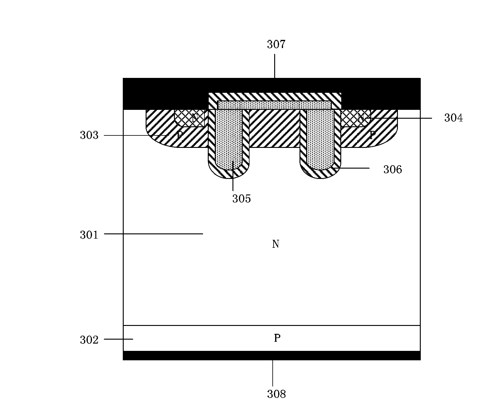
[0115] This embodiment provides another method for forming the IGBT device described in Embodiment 1, including:

[0116] Step S301: Substrate preparation to provide a first semiconductor substrate, the first semiconductor substrate may be N-type doped, or P-type doped, and in this embodiment, the first semiconductor substrate is used as P-type doping is taken as an example to introduce the IGBT device provided by the present invention, but the present invention is not limited thereto.

[0117] Step S302: forming a second semiconductor substrate on the surface of the first semiconductor substrate, the second semiconductor substrate including a drift region 501, in this embodiment, the second semiconductor substrate and the first semiconductor substrate The doping type of the substrate is different, which is N-type doping, and the formation process is preferably an epitaxial process.

[0118] It should be noted that, in one embodiment of the present invention, before forming t...


PUM


Abstract

The embodiment of the invention discloses an IGBT device and a forming method thereof. The IGBT device comprises a semiconductor substrate, a base region, a gate structure, an emitter and a collector. The gate structure includes a U-shaped part and a horizontal part, wherein the U-shaped part of the gate structure penetrates through the base region, the horizontal part of the gate structure covers part of the upper surface of the base region, and the horizontal part and the U-shaped part of the gate structure form an integral structure. The emitter is formed in positions, respectively on the two sides of the U-shaped part of the gate structure, in the base region, and is not in contact with the U-shaped part of the gate structure. Therefore, the IGBT device provided by the invention has the advantages of low difficulty of production technology, low saturated conduction voltage drop, high latch-resistant capability, low saturation current and the like.

Description

technical field [0001] The invention relates to the technical field of semiconductor device manufacturing, in particular to an IGBT device and a forming method thereof. Background technique [0002] Insulated Gate Bipolar Transistor (IGBT for short) is a composite fully-controlled voltage-driven power semiconductor device composed of a bipolar transistor (BJT) and an insulated gate field effect transistor (MOSFET), and has a MOSFET The advantages of the high input impedance of the device and the low conduction voltage drop of the power transistor (that is, the giant transistor, GTR for short), because the IGBT has the advantages of small driving power and low saturation voltage, the IGBT is currently used as a new type of power electronic device It is widely used in various fields. However, the performance of IGBT devices in the prior art is not good. Contents of the invention [0003] In order to solve the above technical problems, an embodiment of the present invention...

Claims


Application Information

Patent Timeline
Patent Type & Authority Applications(China)
IPC IPC(8): H01L29/739H01L29/423H01L21/331
CPCH01L29/0804H01L29/42356H01L29/4236H01L29/66333H01L29/7397H01L29/7398
Inventor 褚为利朱阳军张文亮王波谈景飞
Owner INST OF MICROELECTRONICS CHINESE ACAD OF SCI
Why Eureka
Try Eureka