A carrier-enhanced igbt device with optimized electric field in the body

A carrier, enhanced technology, applied in semiconductor devices, electrical components, circuits, etc., can solve the problems of insufficient turn-off capability, reduced turn-off time, poor reliability, etc., to reduce the impact ionization rate, reduce the turn-off time, the effect of improving withstand voltage and operating reliability

Active Publication Date: 2020-08-28
UNIV OF ELECTRONICS SCI & TECH OF CHINA
View PDF6 Cites 0 Cited by
  • Summary
  • Abstract
  • Description
  • Claims
  • Application Information

AI Technical Summary

Problems solved by technology

[0005] In view of the above, the present invention aims at the insufficient turn-off capability of the existing carrier-enhanced IGBT device, which leads to E off -V cesat To solve problems such as poor compromise and poor reliability, a carrier-enhanced IGBT device with optimized internal electric field is provided, which is equivalent to a variable resistor by introducing gate control into the P+ hole storage layer of the traditional carrier-enhanced IGBT device JFET structure, in order to reduce the turn-off time, reduce the turn-off loss, and obtain better E off -V cesat compromise relationship

Method used


Image

  • A carrier-enhanced igbt device with optimized electric field in the body
  • A carrier-enhanced igbt device with optimized electric field in the body
  • A carrier-enhanced igbt device with optimized electric field in the body

Examples


Embodiment

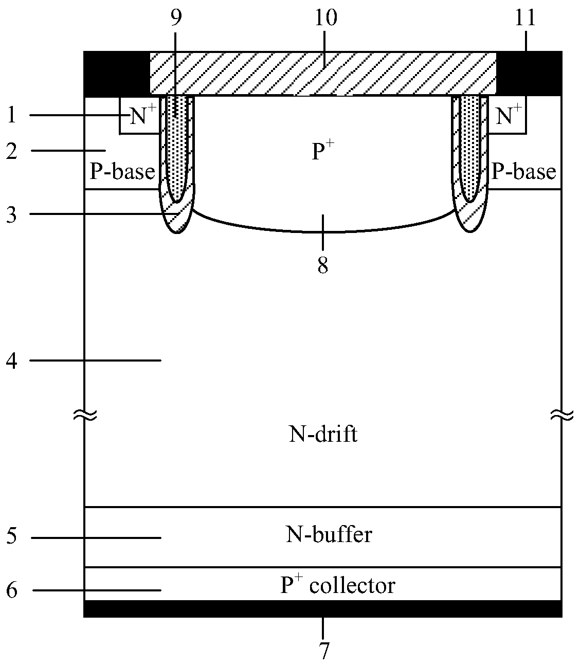
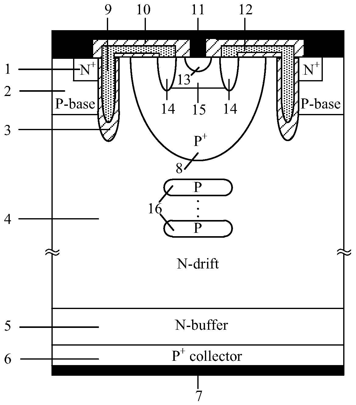
[0029] A carrier-enhanced IGBT device with optimized internal electric field, such as figure 2As shown, its cellular structure includes a metal collector 7, a P+ collector region 6, an N-type buffer layer 5, an N-drift region 4, and a metal emitter 11 stacked sequentially from bottom to top; the N-drift region 4 The middle region of the top layer is provided with a P+ hole storage layer 8, the two sides of the P+ hole storage layer 8 are respectively provided with a P+ base region 2, and the top layer of the P+ base region 2 is provided with an N+ emission region 1; The region 2 and the N+ emitter region 1 are in contact with the P+ hole storage layer 8 through the metal emitter 11; a gate structure is arranged between the P+ base region 2 and the N+ emitter region 1 and the P+ hole storage layer 8, and the The gate structure includes a gate electrode 9 and a gate dielectric layer 3. The gate dielectric layer 3 extends into the N-drift region 4 along the vertical direction of...


PUM


Abstract

The invention relates to a carrier enhanced IGBT device which optimizes the electric field in the body, belonging to the technical field of power semiconductor devices. The present invention introduces a JFET structure equivalent to a variable resistance under gate control into the P+ hole storage layer of a traditional carrier-enhanced IGBT device, so as to reduce the turn-off time and turn-off loss, and obtain a better E off -V cesat Compromise relationship; at the same time, several P-type floating buried layers distributed along the vertical direction of the device are introduced into the N-drift region under the P+ hole storage layer, which is beneficial to reduce the voltage of the P+ hole storage layer when the device is conducting forward, and suppress The parasitic NPN in the JFET structure is turned on, which reduces the impact ionization rate at the bottom of the P+ hole storage layer when the device is turned off, and improves the withstand voltage and operational reliability of the device; the invention proposes that the IGBT device is compatible with the manufacturing process of the existing IGBT device, which is beneficial Realize industrialization.

Description

technical field [0001] The invention belongs to the technical field of power semiconductor devices, and in particular relates to a carrier-enhanced IGBT device that optimizes an internal electric field. Background technique [0002] Insulated Gate Bipolar Transistor (IGBT), as a commonly used field-controlled power device, has many advantages such as high input impedance, fast switching speed, high current density, and low saturation voltage. It is one of the main devices for conversion and conversion, and is widely used in rail transit, new energy vehicles, wind power generation and other fields. [0003] As an important index to measure the design quality of power devices, reducing device loss has attracted much attention of technicians. Among them, the switching loss and the on-state loss are the main parts of the device loss. The on-state loss mainly comes from the large current in the on-state, the saturated conduction voltage drop, and the high voltage and leakage cur...

Claims


Application Information

Patent Timeline
Patent Type & Authority Patents(China)
IPC IPC(8): H01L29/739H01L29/40H01L29/06
CPCH01L29/0623H01L29/402H01L29/7397
Inventor 李泽宏彭鑫杨洋张金平高巍任敏张波
Owner UNIV OF ELECTRONICS SCI & TECH OF CHINA
Why Eureka
Try Eureka