An igbt device with mos controlled hole pathway

A device and path technology, applied in the field of power semiconductor devices, can solve the problems of large switching loss and reduced device withstand voltage, and achieve the effect of reducing the saturated conduction voltage drop, making the manufacturing process compatible, and reducing the turn-off loss.

Active Publication Date: 2021-03-30
UNIV OF ELECTRONICS SCI & TECH OF CHINA
View PDF4 Cites 0 Cited by
  • Summary
  • Abstract
  • Description
  • Claims
  • Application Information

AI Technical Summary

Problems solved by technology

[0005] In view of the foregoing, the present invention provides an IGBT with a MOS-controlled hole path for the existing discrete floating P-region trench gate IGBT devices that have problems such as P-region potential changes resulting in reduced device withstand voltage and large switching losses. device

Method used


Image

  • An igbt device with mos controlled hole pathway
  • An igbt device with mos controlled hole pathway
  • An igbt device with mos controlled hole pathway

Examples


Embodiment 1

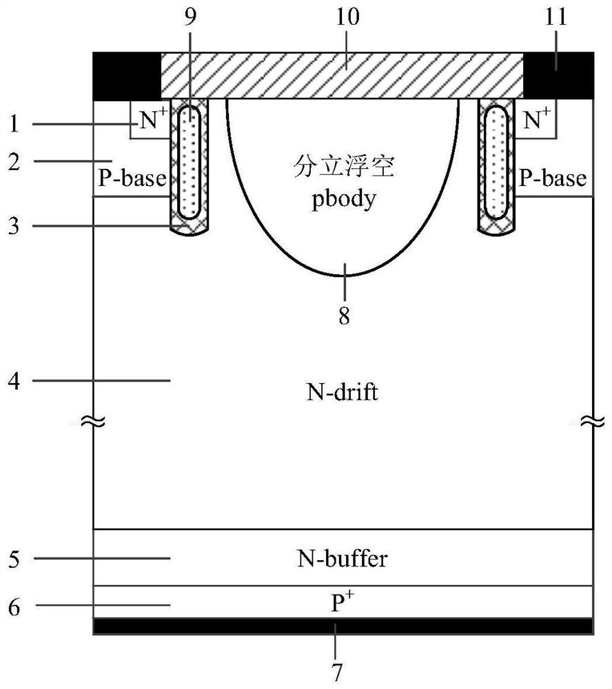
[0033] An IGBT device with a MOS-controlled hole path, such as figure 2As shown, its cell structure includes a metal collector 7, a P+ collector region 6, an N-type buffer layer 5, an N-drift region 4 and a metal emitter 11 stacked in sequence from bottom to top; the N-drift region 4 has A P+ floating pbody region 8 is arranged in the middle area of ​​the top layer, P+ base regions 2 are respectively arranged on both sides of the P+ floating pbody region 8, and an N+ emission region 1 is arranged on the top layer of the P+ base region 2; Region 2 and N+ emitter region 1 are in contact with metal emitter 11; an IGBT gate structure is provided between the P+ base region 2 and N+ emitter region 1 and the P+ floating pbody region 8, and the P+ floating pbody region 8 Not adjacent to the gate structure, the gate structure includes a gate electrode 9 and a gate dielectric layer 3, the gate dielectric layer 3 extends into the N-drift region 4 along the vertical direction of the devi...

Embodiment 2

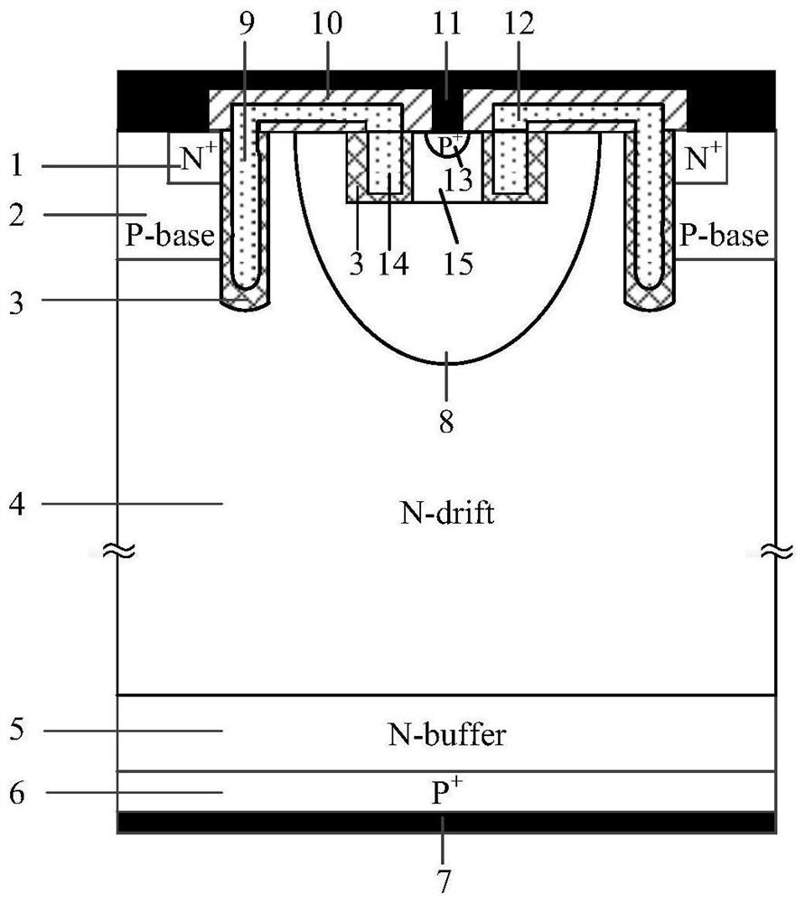
[0052] like image 3 As shown, the difference between this embodiment and Embodiment 1 is that the MOS control gate electrode 14 adopts a sharp-angle MOS control gate structure to further reduce the Miller capacitance.


PUM


Abstract

The invention provides an IGBT device with a MOS-controlled hole path, which belongs to the technical field of power semiconductor devices. The invention introduces a gate dielectric layer, a MOS control gate electrode and a P-type MOS into the P+ floating pbody region of a traditional IGBT device. The MOS control gate structure formed in the channel region, the MOS region is equivalent to a switch controlled by the gate voltage; when the device is forward-conducting, the potential of the pbody region is floating to realize hole storage and reduce the saturation conduction voltage drop of the device ; Under device off and short-circuit conditions, it provides a hole discharge path, reduces Miller capacitance, and achieves low turn-off loss and more stable short-circuit capability.

Description

technical field [0001] The invention belongs to the technical field of power semiconductor devices, and in particular relates to an IGBT device with a MOS-controlled hole path. Background technique [0002] Insulated Gate Bipolar Transistor (IGBT) is widely used in important fields such as rail transit, smart grid, wind power generation, etc. due to its advantages of easy gate drive, high input impedance, high current density, and reduced saturation voltage. It has become one of the mainstream power switching devices in the medium and high power range, and will continue to develop in the direction of high voltage and high current, low power loss, high operating temperature and high reliability. [0003] Planar gate structure is a mature structure often used in high-voltage IGBTs. It is used in environments with high reliability requirements such as high-speed rail and power transportation. However, because of parasitic MOS resistance, planar gate IGBTs have higher saturation...

Claims


Application Information

Patent Timeline
Patent Type & Authority Patents(China)
IPC IPC(8): H01L29/06H01L21/331H01L29/739
CPCH01L29/0619H01L29/083H01L29/1095H01L29/417H01L29/42376H01L29/7397H01L29/4236
Inventor 李泽宏彭鑫赵一尚任敏张波
Owner UNIV OF ELECTRONICS SCI & TECH OF CHINA
Why Eureka
Try Eureka