A kind of insulated gate field effect transistor and its manufacturing method

A technology for field effect transistors and manufacturing methods, which is applied in the field of insulated gate field effect transistors, can solve the problems of poor high-frequency switching characteristics of IGBT, reduce JFET resistance, limit application occasions, etc., and achieve high-frequency switching characteristics and small saturation The conduction voltage drop, the effect of strong practicability

Active Publication Date: 2018-03-30
INST OF MICROELECTRONICS CHINESE ACAD OF SCI +2
View PDF3 Cites 0 Cited by
  • Summary
  • Abstract
  • Description
  • Claims
  • Application Information

AI Technical Summary

Problems solved by technology

[0006] 1. Although JFET injection can reduce the JFET resistance of the device to a certain extent, it also has the risk of reducing the withstand voltage of the device, so this method cannot be used to reduce the JFET resistance blindly.
[0007] 2. JFET implantation is to implant phosphorus ions into the N drift region under the gate between the cells to form a higher concentration of N-type doping. Obviously, such an improvement scheme will cause a reduction in the device withstand voltage
[0008] 3. Because the existing trench IGBT has large input, output and Miller capacitances, the high-frequency switching characteristics of this type of IGBT are not good, which greatly limits its application occasions

Method used


Image

  • A kind of insulated gate field effect transistor and its manufacturing method
  • A kind of insulated gate field effect transistor and its manufacturing method
  • A kind of insulated gate field effect transistor and its manufacturing method

Examples


Embodiment Construction

[0034] In order to further explain the technical means and effects adopted by the present invention to achieve the intended purpose of the invention, the specific implementation and working principle of the insulated gate field effect transistor and its manufacturing method proposed according to the present invention will be described below in conjunction with the accompanying drawings and preferred embodiments. Describe in detail.

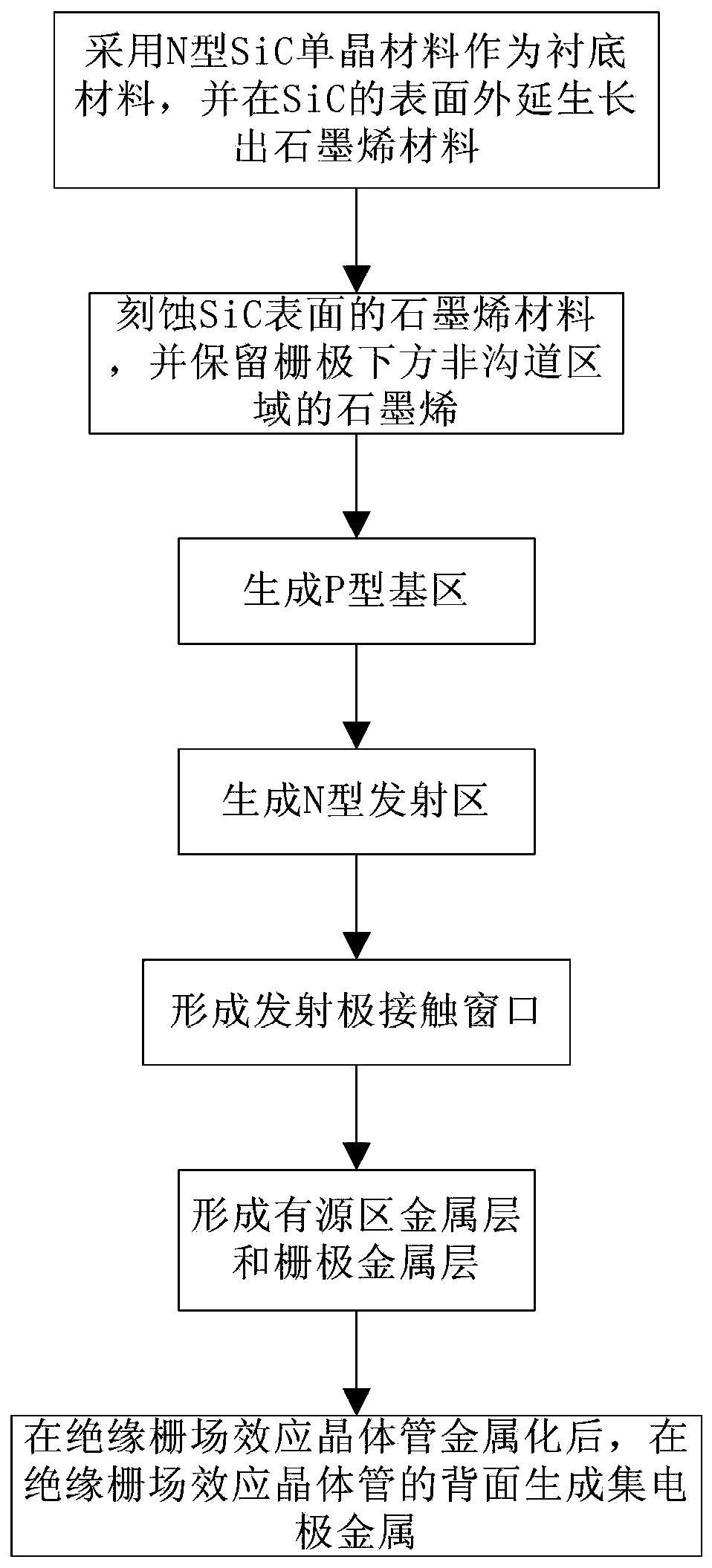
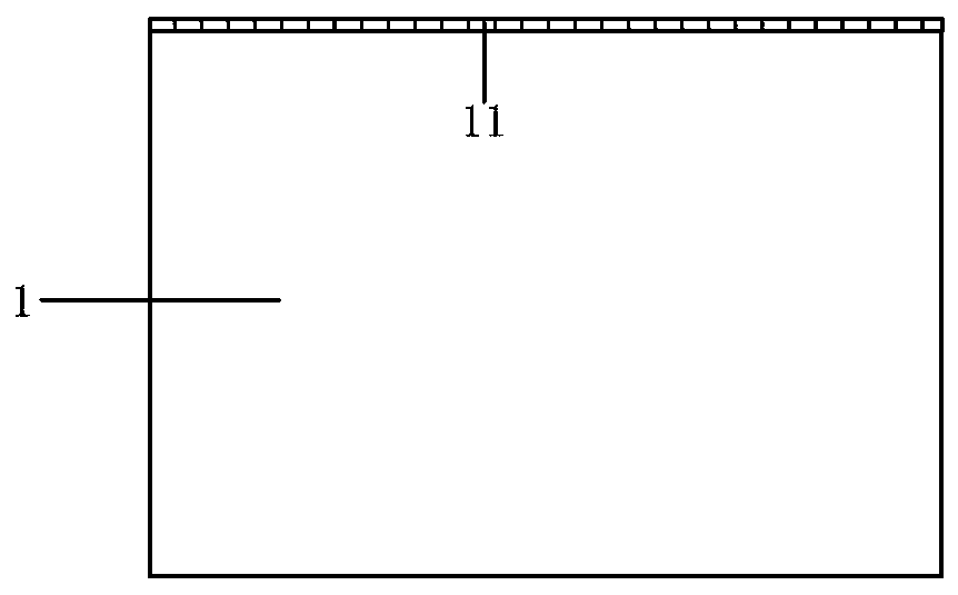
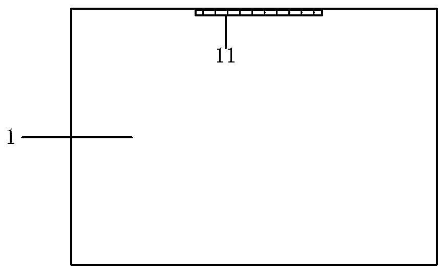
[0035] The insulated gate field effect transistor provided by the present invention includes: a graphene conductive layer; the graphene conductive layer is located between the gate oxide layer and the semiconductor layer in the non-channel region between the cell regions.

[0036] Depend on figure 1 It can be seen that the manufacturing method of the IGSFET provided by the present invention comprises:

[0037] N-type SiC single crystal material is used as the substrate material, and one or more layers of graphene materials are epitaxially grown o...


PUM


Abstract

The invention relates to the technical field of the insulated gate field effect transistor, and discloses an insulated gate field effect transistor and a manufacture method thereof. The manufacture method comprises the following steps: taking N-type SiC monocrystal material as substrate material; carrying out epitaxial growth to graphene on the surface of SiC to form a graphene conducting layer; etching the graphene, and reserving the graphene of a non-channel area between cellular areas below a grid electrode; forming a P-type base area, an N-type emitter area, an active area metal layer and a grid electrode metal layer according to the technology for manufacturing the insulated gate field effect transistor; after the insulated gate field effect transistor is metalized, generating collector metal on the back surface of the insulated gate field effect transistor. According to the invention, on the basis that the voltage endurance of a device is not lowered, the integral resistance of a chip is lowered, and therefore the device has a smaller saturation breakover voltage drop.

Description

technical field [0001] The invention relates to the technical field of an insulated gate field effect transistor, and is mainly applicable to an insulated gate field effect transistor and a manufacturing method thereof. Background technique [0002] As a new type of power electronic device, IGBT is widely used in various occasions. Compared with VDMOS, it has higher current density, lower conduction voltage drop, and higher withstand voltage; compared with power transistors, it has higher withstand voltage and simpler control circuit. and higher switching speeds. However, the pursuit of lower IGBT conduction voltage drop and higher switching speed is a strong demand for the continuous development of power electronic systems. The ways to improve IGBT characteristics can be mainly divided into two aspects: the improvement of device structure and the selection of device materials. First of all, the improvement of the device structure can be divided into the improvement of th...

Claims


Application Information

Patent Timeline
Patent Type & Authority Patents(China)
IPC IPC(8): H01L29/423H01L29/78H01L21/28H01L21/336
CPCH01L29/0603H01L29/66325H01L29/7393
Inventor 褚为利朱阳军卢烁今胡爱斌
Owner INST OF MICROELECTRONICS CHINESE ACAD OF SCI
Why Eureka
Try Eureka