
igbt device with pnp feedthrough transistor

A technology for triodes and devices, applied in the field of power semiconductors, can solve the problems affecting the conduction state of the device, large switching loss, etc., and achieve the effects of reducing leakage current, reducing saturation conduction voltage drop, and increasing breakdown voltage

Active Publication Date: 2020-12-29
UNIV OF ELECTRONICS SCI & TECH OF CHINA
View PDF4 Cites 0 Cited by
  • Summary
  • Abstract
  • Description
  • Claims
  • Application Information

AI Technical Summary

Problems solved by technology

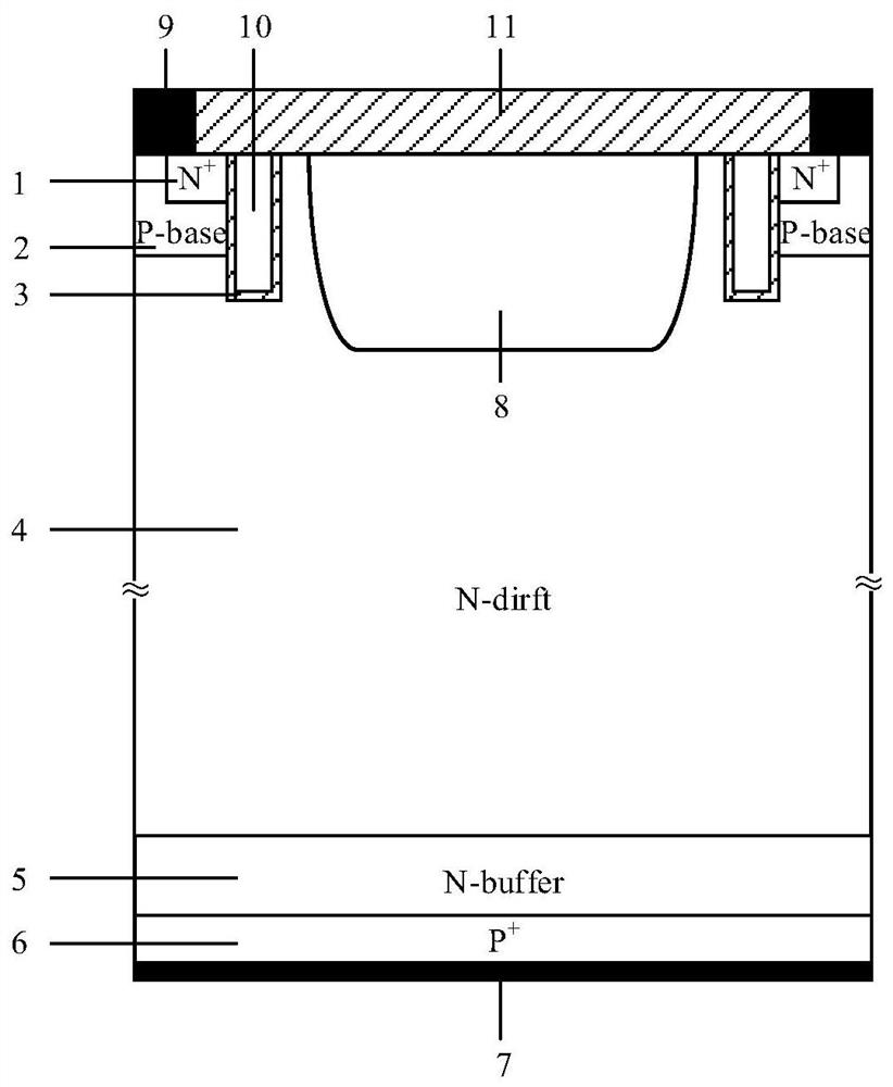
[0005] In view of the above, the present invention aims at the problems existing in the existing trench-gate IGBT devices with discrete floating P-regions that the potential variation of the discrete floating P-regions affects the conduction state, blocking state, and large switching loss of the device, and provides An IGBT device with a PNP feedthrough transistor

Method used


Image

  • igbt device with pnp feedthrough transistor
  • igbt device with pnp feedthrough transistor
  • igbt device with pnp feedthrough transistor

Examples


Embodiment Construction

[0025] Embodiments of the present invention are described below through specific examples, and those skilled in the art can easily understand other advantages and effects of the present invention from the content disclosed in this specification. The present invention can also be implemented or applied through other different specific implementation modes, and various modifications or changes can be made to the details in this specification based on different viewpoints and applications without departing from the spirit of the present invention.

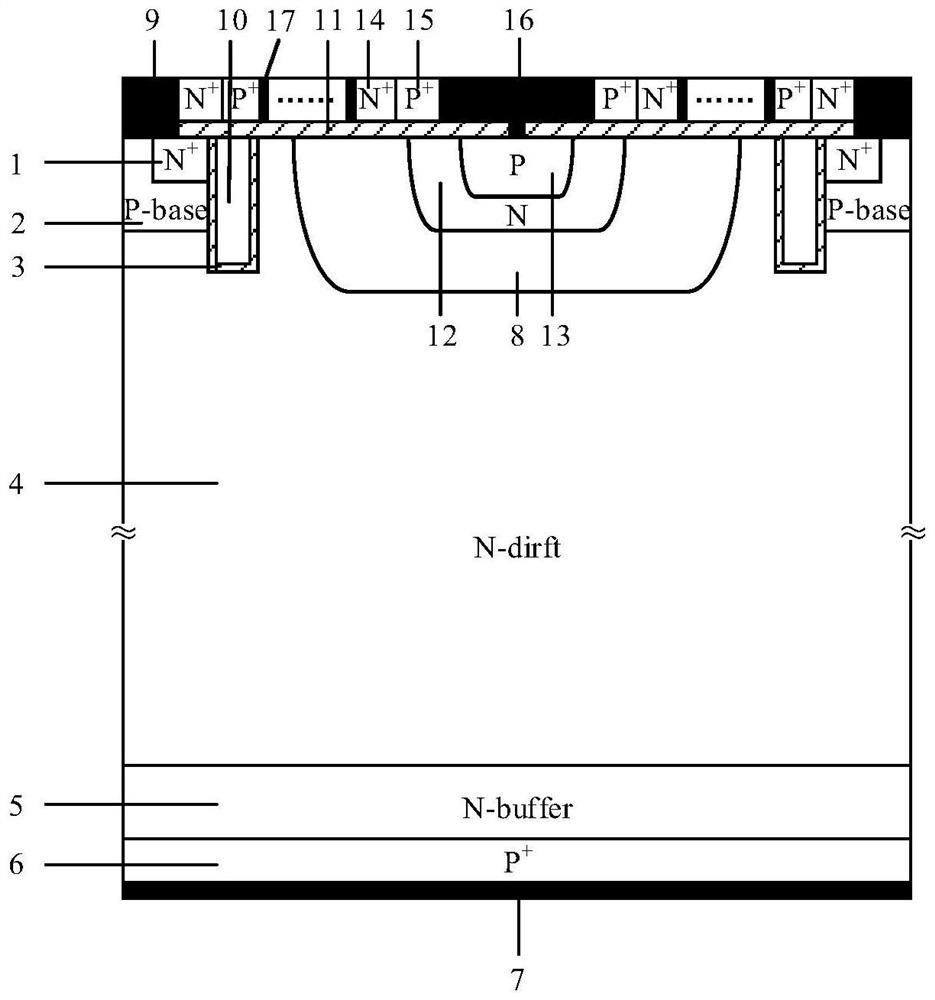
[0026] An IGBT device with a PNP punch-through transistor, the entire cell of which is symmetrical about the cell centerline; the cell structure includes sequentially stacked metal electrodes 7, P+ collector regions 6, N-type buffer layers 5, and N-drift regions from bottom to top 4; the metal emitter 9, the metal electrode 16 and the metal connection 17 are located above the N-drift region 4; the middle region of the top layer of the ...


PUM


Abstract

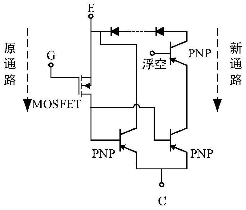
The invention belongs to the technical field of power semiconductors, and specifically relates to an IGBT device with a PNP feed-through transistor. A P-type second collector region, an N-type second base region and a discrete floating Pbody region form a PNP transistor structure; , the PNP triode structure is non-conductive, and stores holes to enhance conductance modulation, and further reduces the leakage current by connecting a diode in series on the metal electrode; when it is turned off, the PNP triode passes through to provide a hole discharge channel, reducing the off time and achieving Without affecting other electrical characteristics, the switching time and switching loss are reduced; when the device is in a blocking state, the PNP transistor breaks through, which increases the withstand voltage capability of the device.

Description

technical field [0001] The invention belongs to the technical field of power semiconductors, and in particular relates to an IGBT device with a PNP punch-through transistor. Background technique [0002] Insulated Gate Bipolar Transistor (IGBT), which is in MOSFET (Metal-Oxide-Semiconductor Field-Effect Transistor, Metal-Oxide Semiconductor Field Effect Transistor) and BJT (Bipolar Junction Transistor, Bipolar Junction Transistor) ) is a new type of composite power device born on the basis of IGBT is widely used in switching power supply, rectifier, inverter, UPS (Uninterruptible Power System, uninterruptible power supply) and other fields due to its advantages of small driving current, high input impedance, good thermal stability, and large working current. At the same time, it is also the basis for the development of new technologies such as rail transportation and solar wind power generation. [0003] Since Baliga of General Electric Company of the United States first p...

Claims


Application Information

Patent Timeline
Patent Type & Authority Patents(China)
IPC IPC(8): H01L29/06H01L29/08H01L29/10H01L29/739H01L27/06
CPCH01L27/0635H01L29/0615H01L29/0638H01L29/0684H01L29/0696H01L29/0821H01L29/1004H01L29/7397H01L29/7398
Inventor 李泽宏孙肇峰何云娇赵一尚莫佳宁杨洋贾鹏飞
Owner UNIV OF ELECTRONICS SCI & TECH OF CHINA
Learn More