
Semiconductor device and manufacturing method thereof
A semiconductor and device technology, applied in the field of semiconductor devices and their production, can solve problems such as poor performance and semiconductor device failure, and achieve the effect of improving performance and avoiding failure
Patent Information
- Authority / Receiving Office
- CN · China
- Patent Type
- Applications(China)
- Current Assignee / Owner
- Publication Date
- 2014-06-11
Smart Images
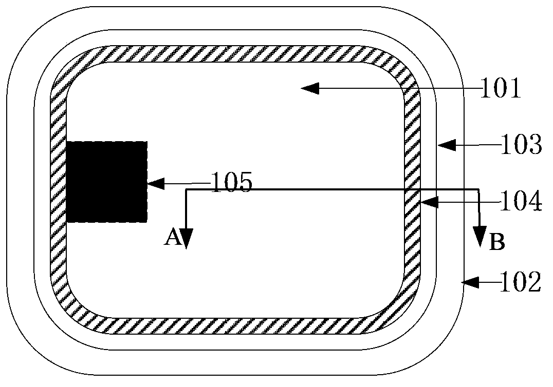
Figure 1 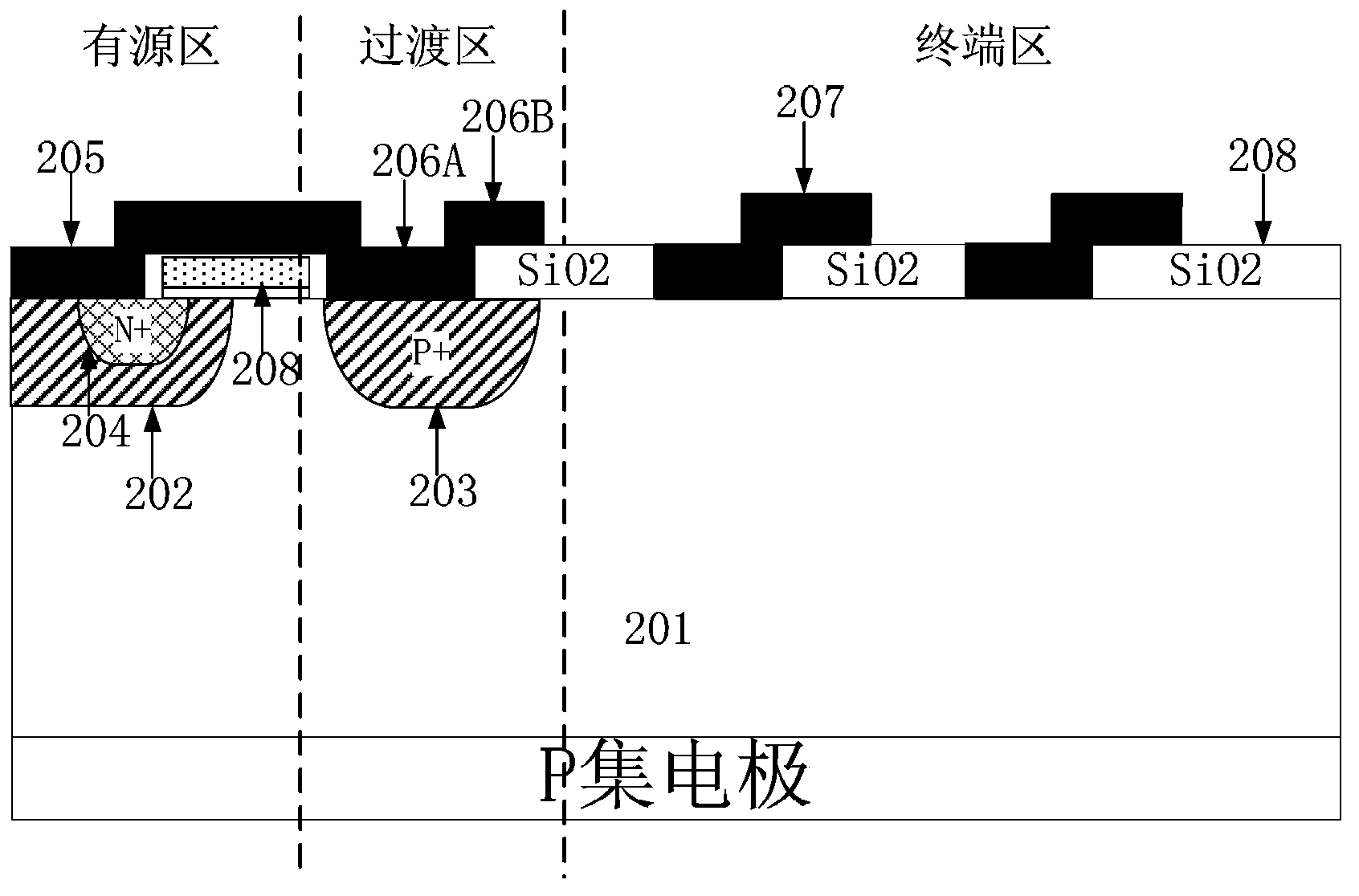
Figure 2 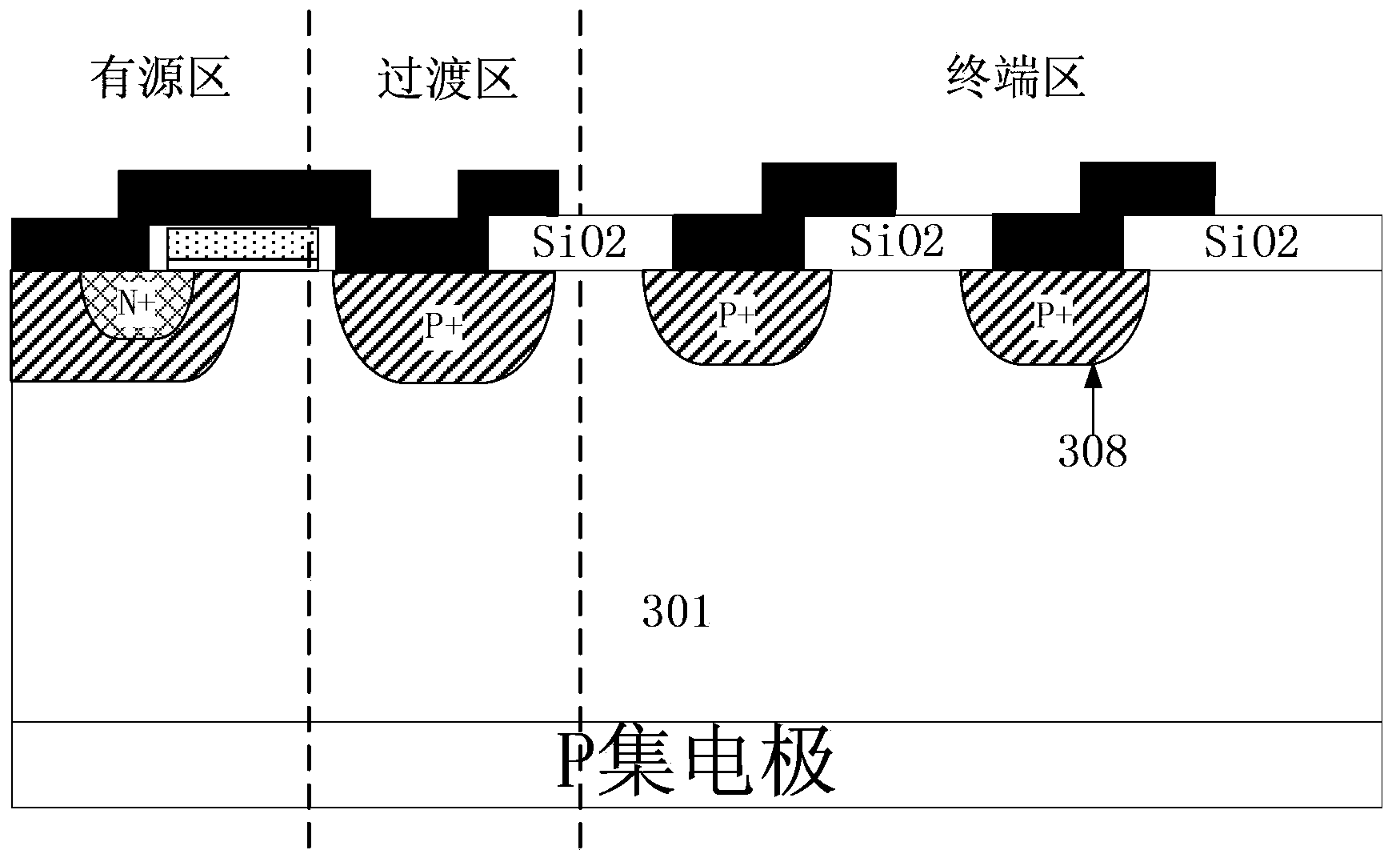
Figure 3
Abstract
Description
technical field
[0001] The invention belongs to the field of semiconductor devices, in particular to a semiconductor device and a manufacturing method thereof. Background technique
[0002] Modern high-voltage semiconductor devices such as IGBT, VDMOS, and power diodes are the third-generation power electronics products. Due to their high operating frequency, fast switching speed, and high control efficiency, they have been more and more widely used in the field of power electronics. The blocking capability of modern high-voltage power semiconductor devices is a very important symbol to measure the development level of semiconductor devices. According to its application, the breakdown voltage ranges from 25V to 6500V. However, due to the planar terminal structure used in modern semiconductor technology, the junction depth Shallow, the edge of the junction is bent, so that the withstand voltage is reduced, the stability of the withstand voltage is poor, the safe working area ...
Examples
Embodiment Construction
[0027] As mentioned in the background section, semiconductor devices in the prior art are prone to failure and have poor performance.
[0028] The inventors found that there are two main reasons why existing semiconductor devices are prone to failure: on the one hand, during the turn-on and turn-off processes of the semiconductor device, the base region close to the main junction in the active region of the semiconductor device is prone to latch-up Lock-in effect, causing semiconductor devices to fail. On the other hand, when the semiconductor device is subjected to a reverse voltage, the main junction of the semiconductor device is prone to premature breakdown, resulting in failure of the semiconductor device.
[0029] The inventors have found that the main reason for the latch-up effect to occur easily in the base region close to the main junction in the active region of the semiconductor device is that there will be a large dynamic avalanche current during the turn-on and t...