Radio-frequency micro-capacitance fingerprint acquisition chip and method

A fingerprint acquisition and capacitance technology, which is used in electrical digital data processing, character and pattern recognition, instruments, etc., can solve the problem that fingerprint sensors cannot meet the special requirements of mobile devices.

Active Publication Date: 2014-06-18
成都费恩格尔微电子技术有限公司 +1
View PDF8 Cites 45 Cited by
  • Summary
  • Abstract
  • Description
  • Claims
  • Application Information

AI Technical Summary

Problems solved by technology

[0009] Therefore, existing fingerprint sensors, no matter capacitive or radio-frequency fingerprint sensors, detect the valley-ridge capacitance difference formed by finger valleys, ridges and sensor sensing electrodes. For existing domestic fingerprint sensors, it is possible to detect The valley ridge capacitance difference is at the order of several fF. For the existing foreign fingerprint sensors, the valley ridge capacitance difference that can be detected is at the order of 0.1fF. The existing domestic and foreign fingerprint sensors cannot meet the special requirements of mobile devices.

Method used


Image

  • Radio-frequency micro-capacitance fingerprint acquisition chip and method
  • Radio-frequency micro-capacitance fingerprint acquisition chip and method
  • Radio-frequency micro-capacitance fingerprint acquisition chip and method

Examples


Embodiment 1

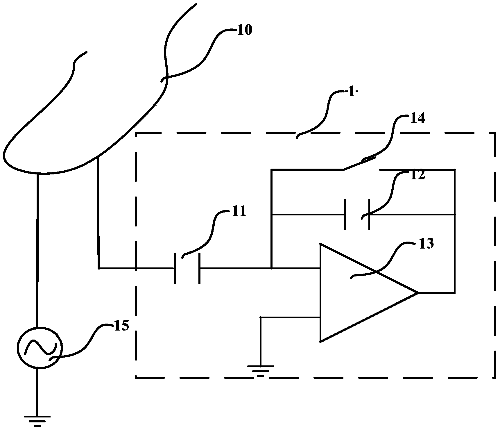
[0143] see Figure 4 , Figure 4 It is a schematic diagram of the circuit structure of the sensing unit in the embodiment of the radio frequency microcapacitance fingerprint sensor chip of the present invention. As shown in the figure, each sensing unit 201 may include: a single sensing electrode 402 formed by a top layer metal formed by an integrated circuit process and a sensing capacitor dielectric layer, which is insulated by the top layer metal 401 Layer structure, a single sensing electrode 401 forms a single sensing capacitor 40 with a finger and a sensing capacitor dielectric layer.

[0144] Besides, each sensing unit 201 also includes a reference capacitor 423 , an active amplifier 44 , a correction capacitor 421 , an enhancement capacitor 420 , a reference capacitor 423 and switch circuits 410 , 411 , 412 , 413 . Among them, a single correction electrode formed by any metal layer of the integrated circuit process, the single correction electrode and a single sensin...

Embodiment 2

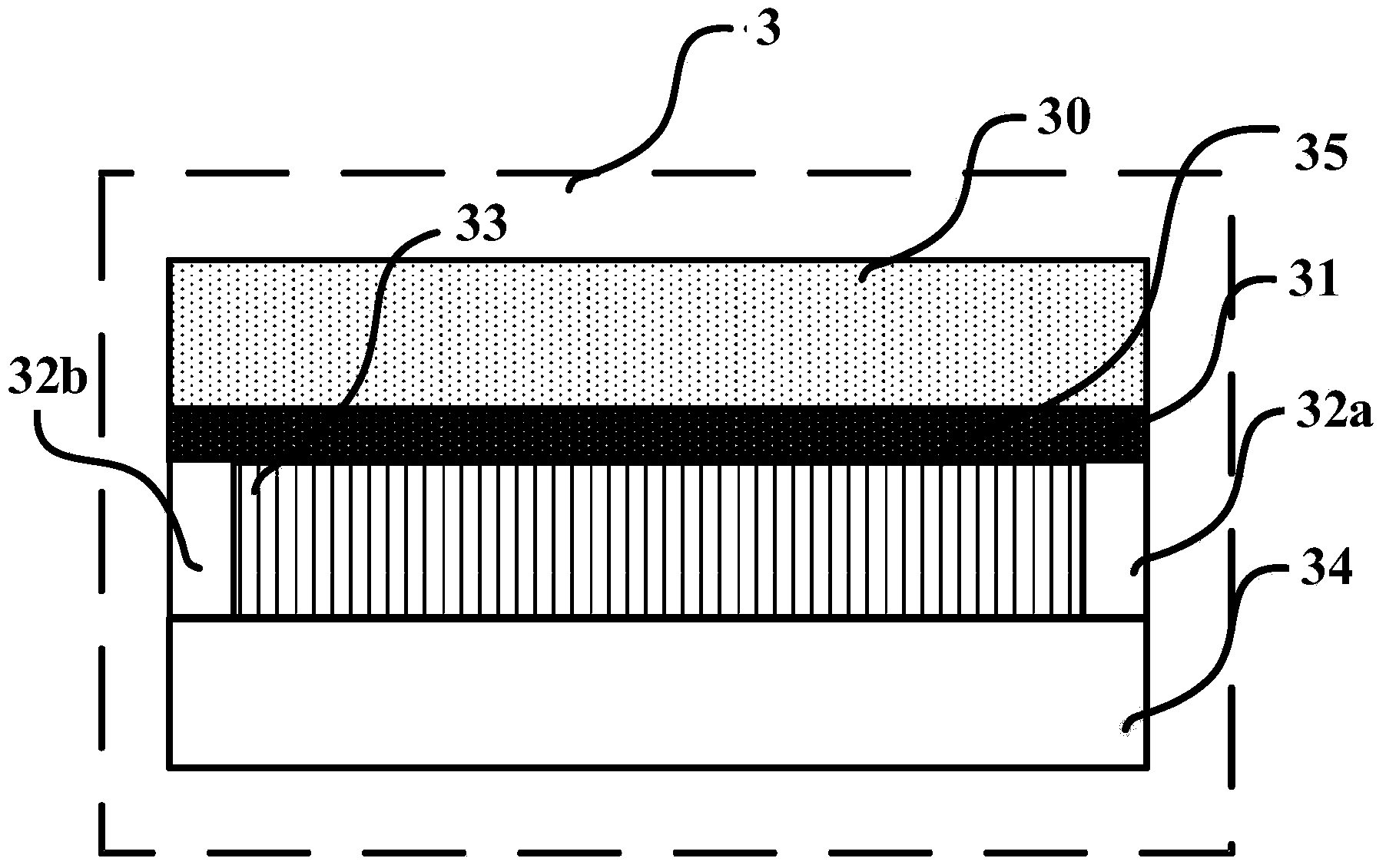
[0182] see Figure 5 , Figure 5 It is a schematic diagram of the circuit structure of the composite sensing unit in the embodiment of the radio frequency microcapacitance fingerprint sensor chip of the present invention. as the picture shows,

[0183] Each composite sensing unit 201 includes optional multiple sub-sensing unit structures; two sensing electrodes 502a and 502b formed by the top layer metal of the integrated circuit process; a sensing capacitor dielectric layer (not shown), which is integrated An insulating layer, a non-conductive adhesive, and an insulating substrate are formed on the top metal of the circuit technology, and two sensing electrodes 502a and 502b form sensing capacitors 50a and 50b with the finger corium layer 501 and the sensing capacitor dielectric layer; Sensing electrodes 502a and 502b form two enhancement capacitors 520a and 520b, two sensing unit offset correction capacitors 521a and 521b, and two shielding capacitors 522a and 522b formed ...


PUM


Abstract

The invention discloses a radio-frequency micro-capacitance fingerprint acquisition chip and method. The chip comprises a plurality of reference sensing units, a two-dimensional sensing unit array formed by the reference sensing units, an insulating layer, an insulating substrate serving as a finger contact surface, a radio-frequency signal generation circuit, a radio-frequency drive electrode, a sensing unit array controller used for providing bias-power-supply switching signals for switching on or switching off the sensing units and charge-discharge sequence signals needed by the sensing units, an analog-digital conversion array, a digital-analog converter for controlling the gain of the analog-digital conversion array, a sensing unit offset correction circuit, a fingerprint image cache, a fingerprint image output controller and an image signal processor. Due to the improvement of the structure of the sensing units and the additional arrangement of the sensing unit offset correction circuit, the radio-frequency micro-capacitance fingerprint acquisition chip can solve the problems of fingerprint residual, interference caused by other radiofrequency radiation, false fingers and small detection depth; besides, the chip can be embedded into a capacitive touch screen.

Description

technical field [0001] The invention relates to the field of integrated circuit design, in particular to a radio frequency microcapacitor fingerprint collection chip and a collection method thereof. Background technique [0002] As people's requirements for information security are getting higher and higher, living biometric authentication and identification are more and more used in people's daily life. Fingerprint authentication has high reliability and cost-effectiveness in biometric authentication, and has become the mainstream of current biometric authentication. At the same time, fingerprint collection technology is also developing rapidly. A fingerprint sensor with lower cost, faster speed, small size, low power consumption, high dynamic range and high detection depth will occupy a huge market. Therefore, the fingerprint sensor with the above advantages Fingerprint sensors have become the focus of current research, and capacitive fingerprint sensors have become one o...

Claims


Application Information

Patent Timeline
Patent Type & Authority Applications(China)
IPC IPC(8): G06K9/00G06F3/044
Inventor 徐启波黄昊
Owner 成都费恩格尔微电子技术有限公司
Why Eureka
Try Eureka