Non-photosensitive polyimide passivation layer manufacturing method

A polyimide, non-photosensitive technology, applied in the production field of non-photosensitive polyimide passivation layer, can solve the problems of long soft-baking time and developing time, reducing equipment production efficiency, and increasing developer metal corrosion Risk and other issues, to eliminate the dependence of soft baking temperature and time, reduce high temperature baking time, and eliminate the effect of causing problems

Active Publication Date: 2014-06-18
SHANGHAI HUAHONG GRACE SEMICON MFG CORP
View PDF4 Cites 2 Cited by
  • Summary
  • Abstract
  • Description
  • Claims
  • Application Information

AI Technical Summary

Problems solved by technology

[0014] In addition, the longer soft-baking time and developing time, on the one hand, reduce the production efficiency of related equipment, and also increase the risk of metal corrosion by the developer

Method used


Image

  • Non-photosensitive polyimide passivation layer manufacturing method
  • Non-photosensitive polyimide passivation layer manufacturing method
  • Non-photosensitive polyimide passivation layer manufacturing method

Examples


Embodiment Construction

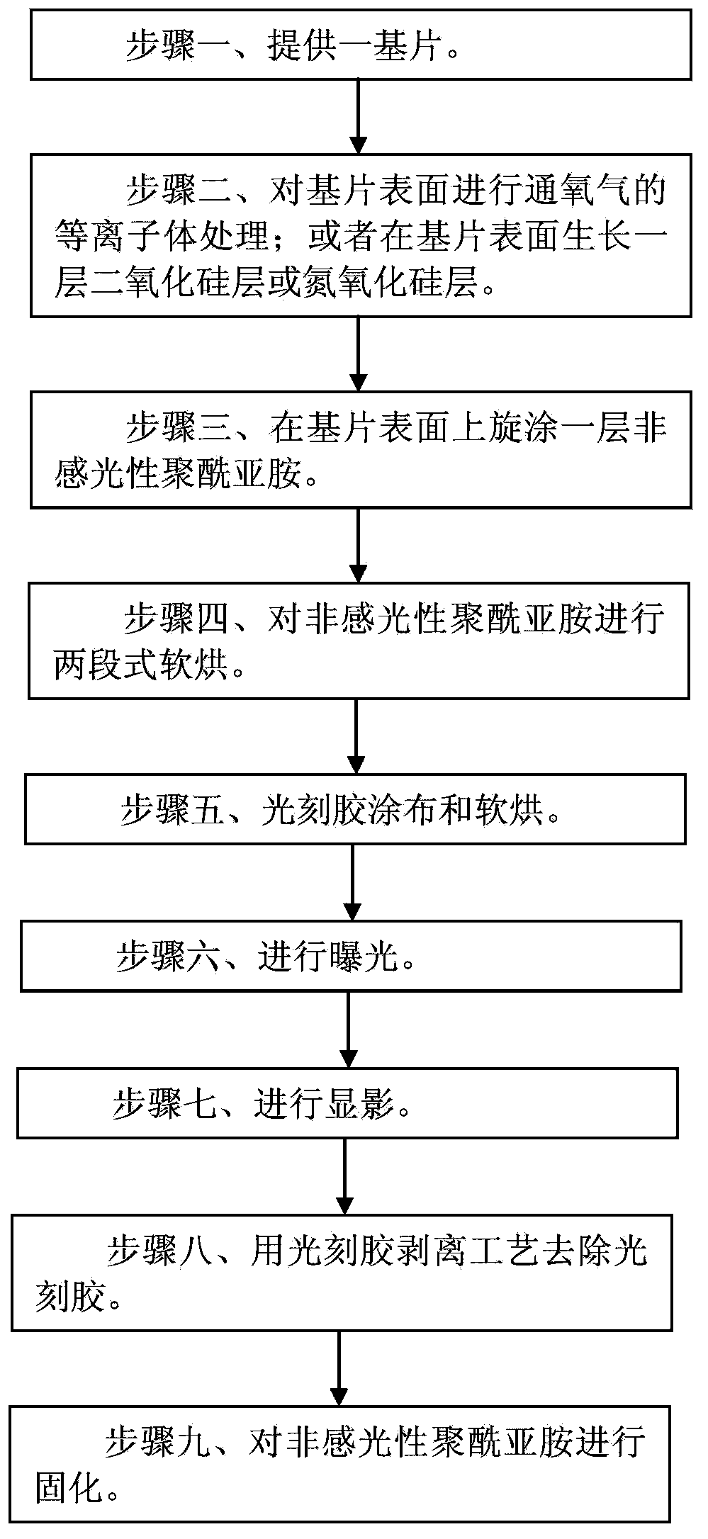
[0045] Such as image 3 Shown is the flow chart of the preparation method of the non-photosensitive polyimide passivation layer of the embodiment of the present invention; the preparation method of the non-photosensitive polyimide passivation layer of the embodiment of the present invention comprises the following steps:

[0046] Step 1, providing a substrate on which a non-photosensitive polyimide passivation layer needs to be fabricated on the surface.

[0047]A semiconductor device is formed in the substrate and the top metal wiring of the semiconductor device has been fabricated, and the non-photosensitive polyimide passivation layer is used to be formed on the top metal wiring and serve as the A passivation layer of a semiconductor device; or, a semiconductor device is formed in the substrate and the top metal wiring of the semiconductor device has been made, and a dielectric layer passivation layer is formed on the top metal wiring, so The non-photosensitive polyimide p...


PUM

PropertyMeasurementUnit
thicknessaaaaaaaaaa
thicknessaaaaaaaaaa
thicknessaaaaaaaaaa

Abstract

The invention discloses a non-photosensitive polyimide passivation layer manufacturing method. The method comprises the following steps of providing a substrate; performing oxygen-filling plasma processing on the surface of the substrate; or growing a silicon dioxide layer or a silicon oxynitride layer on the surface of the substrate; spinning a layer of non-photosensitive polyimide onto the surface of the substrate; baking the non-photosensitive polyimide in two sections to soften the non-photosensitive polyimide; coating a photoresist and baking the photoresist to soften the photoresist; performing development; removing the photoresist by a photoresist stripping process; curing the non-photosensitive polyimide. The problem that the non-photosensitive polyimide is lifted can be solved, the production efficiency can be improved, and the danger that developing liquid corrodes metal during the development is reduced.

Description

technical field [0001] The invention relates to a semiconductor integrated circuit manufacturing process method, in particular to a method for manufacturing a non-photosensitive polyimide passivation layer. Background technique [0002] Because of its excellent heat resistance, chemical corrosion resistance, electrical insulation and mechanical and mechanical properties, polyimide is widely used in chip protection passivation film in microelectronic devices to reduce various natural environments and working conditions. The impact of the environment on semiconductor devices improves the yield of chips and enhances the reliability and stability of devices. With the improvement of the withstand voltage performance of high-voltage devices, the thickness of non-photosensitive polyimide is also required to be higher and higher. . [0003] Such as figure 1 As shown, it is a schematic diagram of the non-photosensitive polyimide after development in the conventional manufacturing m...

Claims


Application Information

Patent Timeline
Patent Type & Authority Applications(China)
IPC IPC(8): H01L21/312G03F7/20G03F7/00
CPCH01L21/31058H01L21/02118
Inventor 程晋广郭晓波童宇锋
Owner SHANGHAI HUAHONG GRACE SEMICON MFG CORP
Why Eureka
Try Eureka