Supercharge Your Innovation With Domain-Expert AI Agents!

Back surface structure of reverse conducting IGBT and manufacturing method thereof

A backside structure, reverse conduction technology, applied in semiconductor/solid-state device manufacturing, semiconductor devices, electrical components, etc., can solve problems such as reduced hole injection efficiency, increased manufacturing costs, wasted chip utilization, and reduced power consumption. , the effect of reducing the conduction voltage drop and avoiding the bounce phenomenon

Active Publication Date: 2014-06-18
INST OF MICROELECTRONICS CHINESE ACAD OF SCI +2
View PDF3 Cites 2 Cited by
  • Summary
  • Abstract
  • Description
  • Claims
  • Application Information

AI Technical Summary

Problems solved by technology

[0007] A reverse conduction type IGBT is also disclosed in the prior art, and the current distribution during forward conduction is as follows: figure 2 As shown, although the bounce phenomenon can be effectively eliminated, but due to the P + Collector area 1 and N + Shorted area 2 is directly adjacent, resulting in part P + Collector region 1 fails to conduct, making P + The hole injection efficiency in the collector region 1 is reduced, which will indirectly waste the utilization rate of the chip and increase the manufacturing cost

Method used


Image

  • Back surface structure of reverse conducting IGBT and manufacturing method thereof
  • Back surface structure of reverse conducting IGBT and manufacturing method thereof
  • Back surface structure of reverse conducting IGBT and manufacturing method thereof

Examples


Embodiment 1

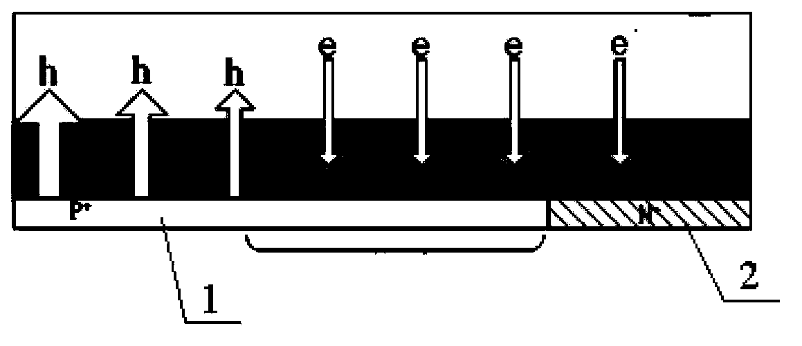
[0044] Such as image 3 As shown, the back structure of a reverse conduction IGBT provided in this embodiment includes: a drift region 100, a first N + Buffer layer 101, P + Collector area 102, N + Short circuit region 103 , insulating layer 104 and collector metal layer 105 . P + The collector region 102 is arranged on one side of the bottom of the drift region 100, N + The short circuit region 103 is set on the other side of the bottom of the drift region 100, P + Collector region 102 and N + The middle of the short-circuit region 103 is separated by a drift region 100, and the drift region 100 is low-doped N - area. P + collector region 102 through the first N + The buffer layer 101 is connected to the drift region 100 . Drift region 100 and first N + The buffer layers 101 are connected to the collector metal layer 105 through the insulating layer 104 . P + The collector region 102 is connected to the collector metal layer 105; N + The depleted part of the sho...

Embodiment 2

[0052] Such as Figure 8 As shown, the back structure of a reverse conduction IGBT provided in this embodiment includes: a drift region 200, a first N + Buffer layer 201, the second N + Buffer layer 206, P + Collector area 202, N + Short circuit region 203 , insulating layer 204 and collector metal layer 205 . P + The collector region 202 is arranged on one side of the bottom of the drift region 200, N + The short circuit region 203 is set on the other side of the bottom of the drift region 200, P + collector area 202 with N + The middle of the short-circuit region 203 is separated by a drift region 200, and the drift region 200 is low-doped N - area. P + collector region 202 through the first N + The buffer layer 201 is connected to the drift region 200 . Drift zone 200, first N + Buffer layer 201 and the second N + The buffer layers 206 are connected to the collector metal layer 205 through the insulating layer 204 . P + The collector region 202 is connected t...


PUM


Abstract

The invention discloses a back surface structure of a reverse conducting IGBT. The back surface structure includes a drift region, a first N+ buffer layer, an insulating layer, a P+ collector region, an N+ short circuit region and a collector electrode metal layer. The P+ collector region is separated from the N+ short circuit region by the drift region in the middle. A depleted part of the N+ short circuit region is connected to the collector electrode metal layer via the insulating layer, and the rest is directly connected to the collector electrode metal layer. The back surface structure and a manufacturing method thereof provided by the utility model add the low-doped drift region of an N- region between the P+ collector region and the N+ short circuit region, so that the P+ collector region is more positively biased, and thus rebounding phenomena are avoided. Besides, the back structure can increase the effective conducting area of the P+ collector region and the total injection of a cavity, reduces conductive voltage drop, and thus reduces power consumption.

Description

technical field [0001] The invention relates to the technical field of power semiconductor devices, in particular to a back structure of a reverse conduction type IGBT and a preparation method thereof. Background technique [0002] The reverse conduction IGBT is a new type of power device, which has many advantages but also introduces some disadvantages, such as bounce phenomenon. [0003] By comparison, it can be found that most of the structure of the reverse conduction IGBT is similar to that of the traditional IGBT. The biggest difference is that the collector of the reverse conduction IGBT is not a continuous P + area, but intermittently introduce some N + short circuit area. [0004] P of the reverse conduction IGBT - base area, N - Drift zone, N + buffer layer and N + The shorted area forms a PIN diode. The reverse conduction IGBT is equivalent to an IGBT and a PIN diode in antiparallel connection, but it is realized on the same chip. When the IGBT is under r...

Claims


Application Information

Patent Timeline
IPC IPC(8): H01L29/739H01L29/06H01L21/331
CPCH01L29/0615H01L29/0821H01L29/66325H01L29/7393
Inventor 张文亮田晓丽朱阳军胡爱斌
Owner INST OF MICROELECTRONICS CHINESE ACAD OF SCI
Features
  • R&D
  • Intellectual Property
  • Life Sciences
  • Materials
  • Tech Scout
  • Unparalleled Data Quality
  • Higher Quality Content
  • 60% Fewer Hallucinations
Learn More