Rear surface passivation contact battery electrode structure and preparation method thereof

A technology of back passivation and battery electrodes, which is applied in the field of solar cells, can solve the problems of expensive metal electrodes, the inability to take advantage of the potential advantages of N-type batteries, and the reduction of battery costs, achieving high pass rate, reduced shading area, and production methods simple effect

Inactive Publication Date: 2016-08-17
LONGI SOLAR TECH CO LTD
View PDF5 Cites 23 Cited by
  • Summary
  • Abstract
  • Description
  • Claims
  • Application Information

AI Technical Summary

Problems solved by technology

However, due to the use of fully covered metal electrodes on the back electrode of the back passivated contact cell, the potential advantages of N-type cells that can generate electricity on both sides cannot be utilized, and the price of metal electrodes is expensive, which is not conducive to the reduction of battery costs.

Method used


Image

  • Rear surface passivation contact battery electrode structure and preparation method thereof
  • Rear surface passivation contact battery electrode structure and preparation method thereof
  • Rear surface passivation contact battery electrode structure and preparation method thereof

Examples


preparation example Construction

[0031] The preparation method of the above-mentioned backside passivation contact battery backside structure comprises the following steps:

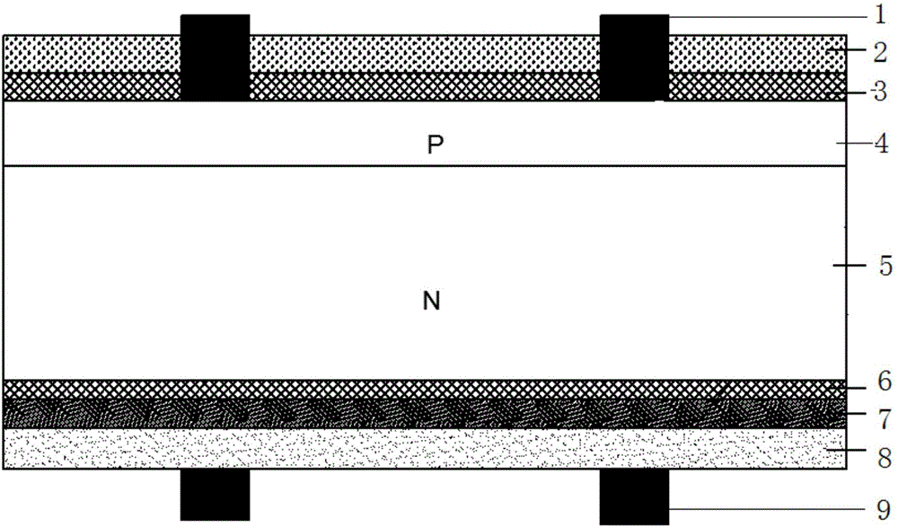
[0032] 1) The N-type crystalline silicon wafer is processed by texturing, diffusion, etching, passivation film and anti-reflection film on the front side, and then the back electrode of the battery is made according to the following steps.

[0033] 2) Fabricate a tunneling silicon oxide film 6 on the back of the N-type crystalline silicon wafer with a film thickness of 1-2nm. The fabrication methods can be LPCVD, PECVD, ALD, thermal oxidation, ozone oxidation, wet chemistry, electrochemical, anodic oxidation, etc. .

[0034] 3) An N-type doped crystal silicon layer 7 is fabricated on the tunneling silicon oxide, and the thickness of this layer is 10-1000 nm. Manufacturing method: ①Using LPCVD and vapor phase epitaxy to directly form N-type doped crystalline silicon layer 7; ②Using PECVD method to first form N-type doped amorphous silico...

Embodiment 1

[0042] (1) N-type crystalline silicon wafers are processed by texturing, diffusion, etching, passivation film and anti-reflection film on the front side, and then the back electrode is made according to the following steps.

[0043] (2) Fabricate a tunneling silicon oxide layer with a thickness of 2nm on the back side by LPCVD.

[0044] (3) An N-type doped microcrystalline silicon layer with a thickness of 30 nm is fabricated on the tunneling silicon oxide layer by LPCVD.

[0045] (4) Sputtering is used to fabricate an ITO transparent conductive film with a thickness of 100 nm on the N-type doped microcrystalline silicon layer.

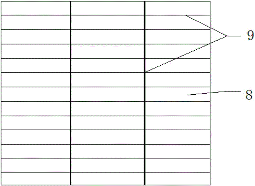
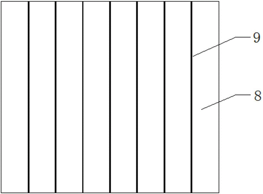
[0046] (5) Fabricate silver electrodes on the transparent conductive film by inkjet method, followed by heat treatment. The silver electrode is composed of a group of equally spaced and parallel thin grid lines and a group of equally spaced parallel main grid lines, and the thin grid lines and the main grid lines are vertically intersected. There ar...

Embodiment 2

[0049] (1) N-type crystalline silicon wafers are processed by texturing, diffusion, etching, passivation film and anti-reflection film on the front side, and then the back electrode is made according to the following steps.

[0050] (2) Fabricate a tunnel silicon oxide film with a thickness of 1 nm on the back side by PECVD.

[0051] (3) An N-type doped amorphous silicon layer with a thickness of 50 nm is fabricated on the tunneling silicon oxide film by PECVD.

[0052] (4) Perform annealing at 200-500°C under a protective atmosphere to convert doped amorphous silicon into microcrystalline silicon;

[0053] (5) AZO transparent conductive film with a thickness of 150 nm was fabricated on the N-type doped microcrystalline silicon layer by sputtering.

[0054] (6) A silver electrode is fabricated on the transparent conductive film by screen printing, followed by heat treatment. The silver electrode is composed of 10 sets of grid lines parallel to each other at equal intervals, ...


PUM


Abstract

The invention discloses a rear surface passivation contact battery electrode structure and a preparation method thereof. A battery back structure comprises a tunneling layer which is arranged on the rear surface of a crystal silicon wafer and used for providing a passivation effect on the rear surface of a battery, the tunneling layer is provided with an N type doped crystal silicon layer used for a charge vertical conducting layer, the N type doped crystal silicon layer is provided with a transparent conducting film for an electric charge horizontal conducting layer, and the transparent conducting film is provided with a rear surface metal electrode for electric charge collection and a connection effect between battery pieces. According to the rear surface passivation contact battery electrode structure, the transparent conducting film / metal combination electrode is adopted so as to replace a conventional grid line electrode or an all metal back field electrode, so that the rear surface of the battery can serve as a light receiving surface, a shading area and the usage amount of conductive metal are remarkably reduced on the premise of guaranteeing good conductivity of the electrode, and the conversion efficiency of the battery is improved.

Description

technical field [0001] The invention belongs to the technical field of solar cells, and in particular relates to a rear passivation contact cell electrode structure and a preparation method thereof. Background technique [0002] Since the first solar cell was born in Bell Laboratories in 1954, crystalline silicon solar cells have been widely used, the conversion efficiency has been continuously improved, and the production cost has continued to decline. At present, crystalline silicon solar cells account for more than 80% of the total global solar cell market, and the conversion efficiency of crystalline silicon cell production lines has exceeded 20%. The cost of electricity continues to shrink and is expected to be flat in the next few years. As a clean energy source, crystalline silicon solar cells play an increasingly important role in changing the energy structure and alleviating environmental pressure. [0003] According to the doping type of the substrate, crystallin...

Claims


Application Information

Patent Timeline
Patent Type & Authority Applications(China)
IPC IPC(8): H01L31/0224H01L31/18
CPCH01L31/022466H01L31/1884Y02P70/50
Inventor 李华赵科雄
Owner LONGI SOLAR TECH CO LTD
Why Eureka
Try Eureka