Light Emission Control Circuit

A light-emitting control circuit and light-emitting control unit technology, applied to instruments, static indicators, etc., can solve the problems of complex circuit design and affect the overall design of the display panel, and achieve the effect of simplifying the design

Active Publication Date: 2014-06-25
AU OPTRONICS CORP
View PDF5 Cites 9 Cited by
  • Summary
  • Abstract
  • Description
  • Claims
  • Application Information

AI Technical Summary

Problems solved by technology

When the driving circuit of the active matrix OLED display provides more control voltages, its circuit design will be more complicated, which will affect the overall design of the display panel

Method used


Image

  • Light Emission Control Circuit
  • Light Emission Control Circuit
  • Light Emission Control Circuit

Examples


Embodiment Construction

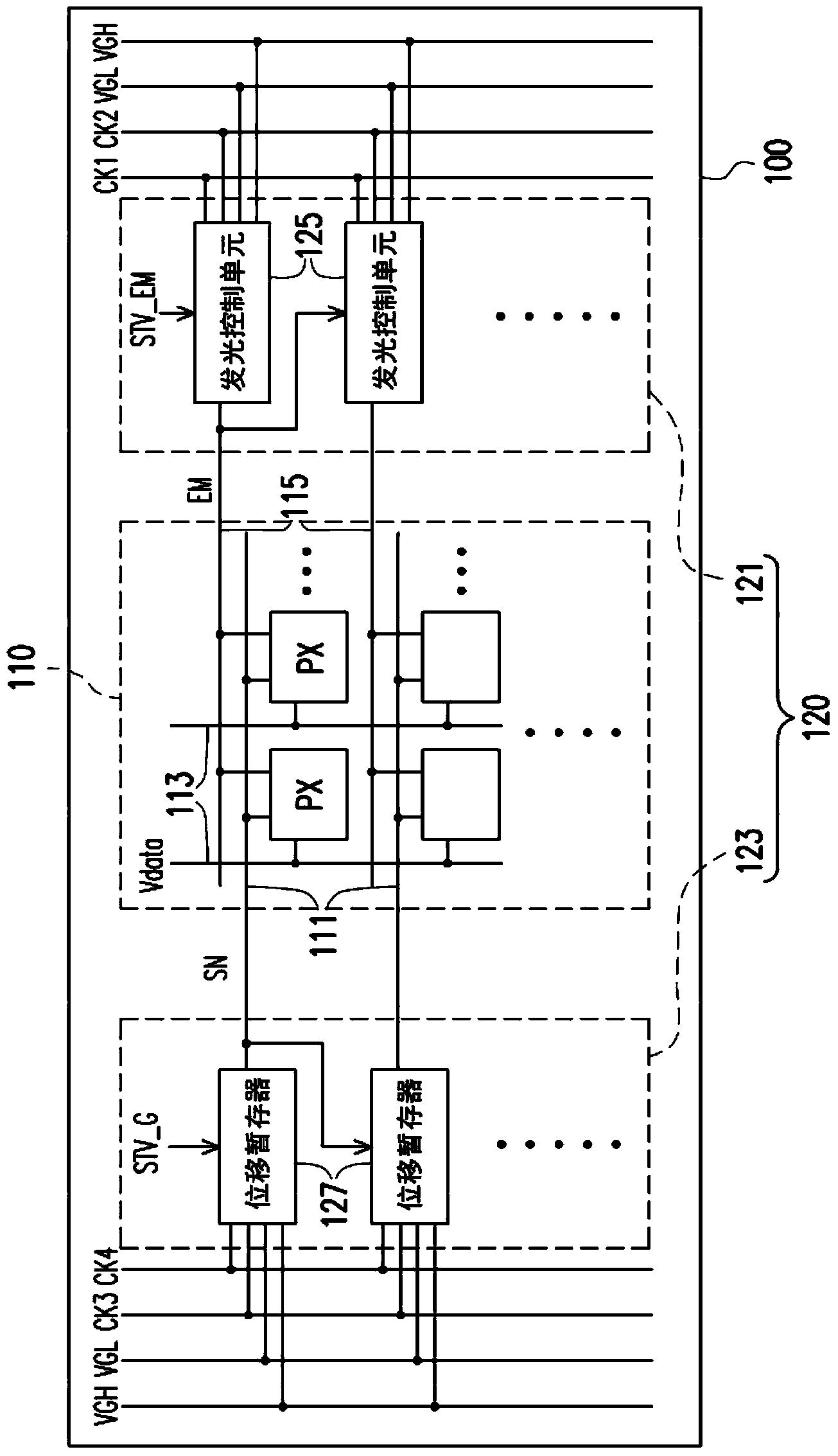
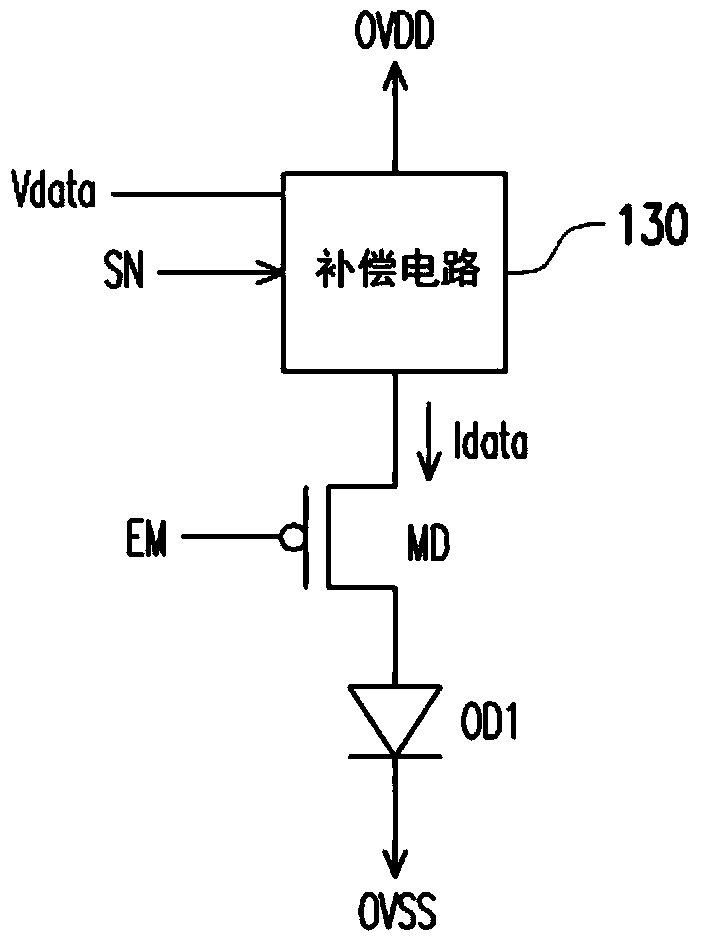
[0050] Figure 1A It is a system diagram of an active matrix organic light emitting diode display panel according to an embodiment of the present invention. Please refer to Figure 1A , in this embodiment, the active matrix OLED display panel 100 includes a pixel array 110 and a driving circuit 120 , wherein the driving circuit 120 includes a light emitting control circuit 121 and a gate driving circuit 123 . The light emitting control circuit 121 is used for providing a plurality of light emitting signals EM, and the gate driving circuit 123 is used for providing a plurality of gate driving signals SN.

[0051]The pixel array 110 includes a plurality of pixels PX, a plurality of scan lines 111 , a plurality of data lines 113 and a plurality of light emission control lines 115 . Each scan line 111 is coupled between the corresponding pixel PX and the gate driving circuit 123 to transmit the corresponding gate driving signal SN to the corresponding pixel PX. Each data line 113...


PUM


Abstract

The present invention discloses a light emission control circuit applied to an active matrix organic light emitting diode display panel. The light emission control includes multiple light emission control units which respectively receive first clock signals second clock signals, high voltage grids and low voltage grids as well as provide multiple light emission signals for multiple pixels of the active matrix organic light emitting diode display panel. The first light emission control unit receives a glowing start signal, the rest light emission control units are respectively the light emission signals provided by the prior light emission control units. The pulse width of the light emission signal is proportional to that of the glowing start signal.

Description

technical field [0001] The present invention relates to a control circuit, and in particular to a lighting control circuit of an OLED display panel. Background technique [0002] Organic Light Emitting Diode (OLED) has the advantages of self-luminescence, high response speed, power saving, light and thin, wide viewing angle, wide color gamut, low operating voltage, high contrast, etc., and the manufacturing process is simple and low cost, and can be applied to Features such as flexible panels have been regarded as one of the most promising flat-panel display technologies in the future after thin film transistor liquid crystal display (TFT LCD). [0003] OLED displays can be roughly classified into passive matrix OLED displays and active matrix OLED displays. The main driving method of the active matrix OLED display is to use thin film transistor (TFT) elements, and use capacitors to store different data voltages, so as to control the gray scale of each pixel on the panel. ...

Claims


Application Information

Patent Timeline
Patent Type & Authority Applications(China)
IPC IPC(8): G09G3/32G09G3/3225G09G3/3266
Inventor 叶荫平
Owner AU OPTRONICS CORP
Why Eureka
Try Eureka