TFT array substrate and manufacture method thereof
A technology of array substrate and manufacturing method, which is applied in the field of thin film transistor array substrate and its manufacturing, and can solve the problems of lower transmittance, liquid crystal alignment disorder, influence, etc.
- Summary
- Abstract
- Description
- Claims
- Application Information
AI Technical Summary
Problems solved by technology
Method used
Image

Examples
Embodiment Construction
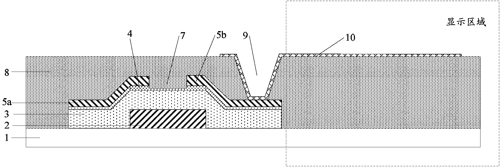
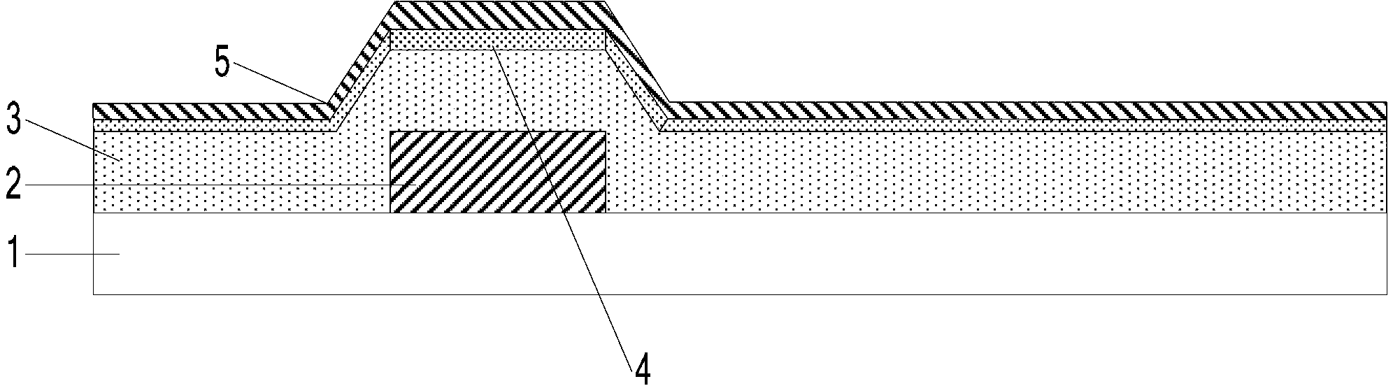
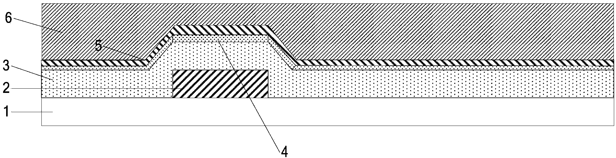
[0037] Since the TFT as a whole will become flat after using the organic resin, the cell rubbing process can be more easily controlled, and the refractive index of the organic resin is basically the same as that of the substrate. Therefore, the organic resin used in the present invention can be used as a flattening material, and can improve the transmittance of the TFT array substrate.
[0038] A thin film transistor TFT array substrate, comprising: a base substrate, TFTs formed on the base substrate, gate lines, data lines, and pixel electrodes, wherein, on the TFT array substrate except the TFT area, Structures other than the gate lines, data lines and pixel electrodes are all formed using organic resin.
[0039] Here, the thin film transistor TFT array substrate further includes: a gate insulating layer; wherein, the gate insulating layer includes: a gate insulating layer formed on the TFT region;
[0040] The thin film transistor TFT array substrate may also include: a pa...
PUM
 Abstract
Description
Claims
Application Information
 - R&D
- Intellectual Property
- Life Sciences
- Materials
- Tech Scout
- Unparalleled Data Quality
- Higher Quality Content
- 60% Fewer Hallucinations
Browse by: Latest US Patents, China's latest patents, Technical Efficacy Thesaurus, Application Domain, Technology Topic, Popular Technical Reports.
© 2025 PatSnap. All rights reserved.Legal|Privacy policy|Modern Slavery Act Transparency Statement|Sitemap|About US| Contact US: help@patsnap.com