
Shielding case and manufacturing method thereof
A technology of shielding cover and insulating cover, applied in the fields of magnetic field/electric field shielding, electrical components, etc., can solve the problems of high mold cost, mold maintenance cost, high mold allocation cost, and high assembly cost, and achieve low assembly cost and low processing cost. , the effect of low cost
- Summary
- Abstract
- Description
- Claims
- Application Information
AI Technical Summary
Problems solved by technology
Method used
Image

Examples
Embodiment Construction
[0025] The present invention will be described in further detail below in conjunction with the accompanying drawings.
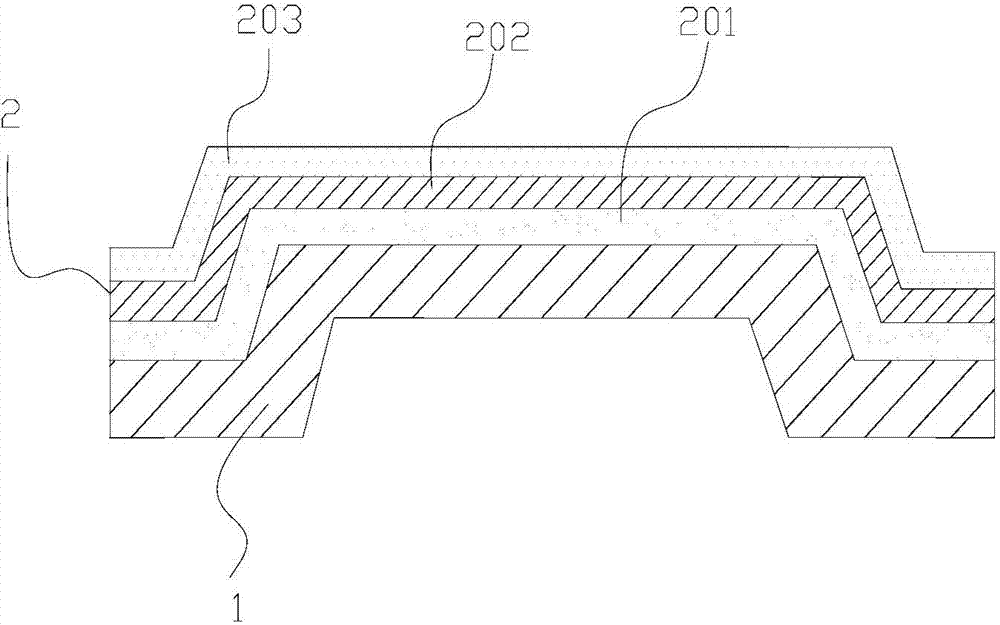
[0026] refer to figure 1 The present invention provides a shielding cover, which includes an insulating cover body 1 and a metal conductive layer 2 arranged on the outer side of the insulating cover body 1, and the thickness of the metal conductive layer 2 is 0.001-0.003 mm. The insulating cover body 1 is made of PS or PC. The thickness of the insulating cover 1 is 0.3-1.6 millimeters. The metal conductive layer 2 includes a first metal layer 201, a second metal layer 202 and a third metal layer 203, the first metal layer 201 is a nickel layer, the second metal layer 202 is a copper layer, and the third metal layer 203 is a silver layer or 18K gold layer, the first metal layer 201 covers the outer side of the insulating cover 1 , the second metal layer 202 covers the first metal layer 201 , and the third metal layer 203 covers the second metal layer 202 . ...
PUM
 Abstract
Description
Claims
Application Information