
LED fluorescent lamp and installation method thereof

A technology of LED fluorescent lamps and glass inner tubes, applied in light sources, electric light sources, electric light sources, etc., can solve problems such as poor compatibility of fluorescent lamp holders

Inactive Publication Date: 2014-07-02
李文雄 +1
View PDF9 Cites 8 Cited by
  • Summary
  • Abstract
  • Description
  • Claims
  • Application Information

AI Technical Summary

Problems solved by technology

In addition, the design of the above-mentioned LED fluorescent lamp completely abandons the shackles of the original fluorescent lamp holder. Although this is conducive to optimizing the structure and circuit design of the fluorescent lamp, it is not compatible with the existing fluorescent lamp holder.

Method used


Image

  • LED fluorescent lamp and installation method thereof
  • LED fluorescent lamp and installation method thereof
  • LED fluorescent lamp and installation method thereof

Examples


Embodiment Construction

[0074] The present invention will be described more fully hereinafter with reference to the accompanying drawings, in which exemplary embodiments of the invention are shown. This invention may, however, be embodied in different forms and should not be construed as limited to only the embodiments set forth herein. The given above-mentioned embodiments are intended to make the disclosure herein comprehensive and complete, and to more fully convey the protection scope of the present invention to those skilled in the art.

[0075] In this specification, unless otherwise specified, the term "semiconductor wafer" refers to a plurality of independent individual circuits formed on a semiconductor material (such as silicon, gallium arsenide, etc.), a "semiconductor wafer" or "die ” refers to such individual circuits, while “packaged chip” refers to the packaged physical structure of a semiconductor die, typically such as mounted on a carrier and encapsulated with an encapsulant.

[00...


PUM


Abstract

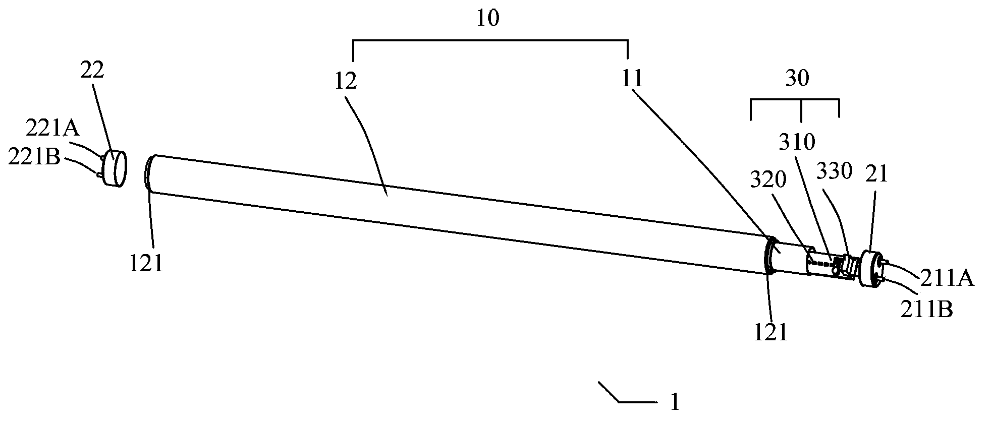
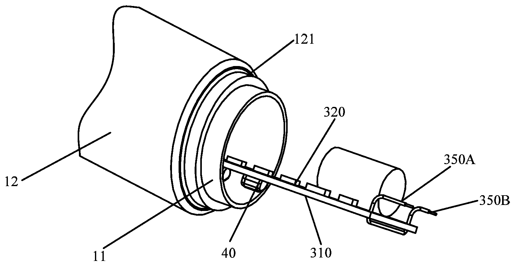
The invention relates to the semiconductor lighting technology, in particular to an LED fluorescent lamp and an installation method thereof. The LED fluorescent lamp according to embodiments comprises a glass inner tube, a glass outer tube enclosing the glass inner tube, end covers covering two ends of the glass inner tube, an LED drive power source, a plurality of LED units, and a drive circuit module; each end cover is provided with pins adapting to a fluorescent lamp holder; the LED drive power source comprises an elongated substrate fixed within the glass inner tube; the drive circuit module is arranged at one end or two ends of the elongated substrate and electrically connected with the LED units and the pins.

Description

technical field [0001] The invention relates to semiconductor lighting technology, in particular to an LED fluorescent lamp and a method for installing the fluorescent lamp. Background technique [0002] The light-emitting diode (LED) currently used as a light source in lighting devices is a solid-state semiconductor device. Its basic structure generally includes a bracket with leads, a semiconductor wafer placed on the bracket, and packaging materials that seal the wafer around. (such as silicone or epoxy). The above-mentioned semiconductor wafer contains a P-N structure. When the current passes through, electrons are pushed to the P region, and in the P region, the electrons recombine with the holes, and then emit energy in the form of photons, and the wavelength of light is formed by the material forming the P-N structure. decided. [0003] Compared with traditional fluorescent lamps, LED fluorescent lamps have many advantages such as high photoelectric conversion effic...

Claims


Application Information

Patent Timeline
Patent Type & Authority Applications(China)
IPC IPC(8): F21S2/00F21V17/10F21V23/06H05B37/02F21Y101/02F21K9/27F21K9/278F21Y115/10
Inventor 李文雄赵依军
Owner 李文雄
Learn More