Glass substrate for display device and method for manufacturing same

A technology for glass substrates and displays, applied in the field of glass substrates for oxide semiconductor thin film transistors) displays, glass substrates for displays and its manufacture, glass substrates for flat panel displays, low temperature polysilicon thin film transistors) glass substrates for displays, and can solve problems , heat shrinkage reduction and other issues

Active Publication Date: 2014-07-09
AVANSTRATE INC
View PDF10 Cites 25 Cited by
  • Summary
  • Abstract
  • Description
  • Claims
  • Application Information

AI Technical Summary

Problems solved by technology

In addition, the technology of Patent Document 3 is insufficient for reducing the thermal...

Method used


Image

  • Glass substrate for display device and method for manufacturing same
  • Glass substrate for display device and method for manufacturing same
  • Glass substrate for display device and method for manufacturing same

Examples


Embodiment

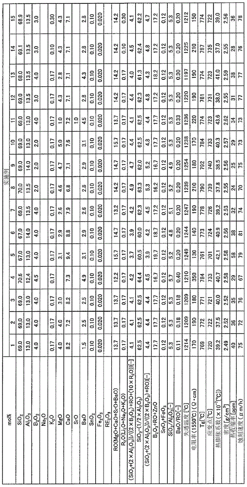
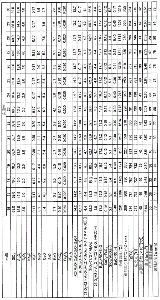
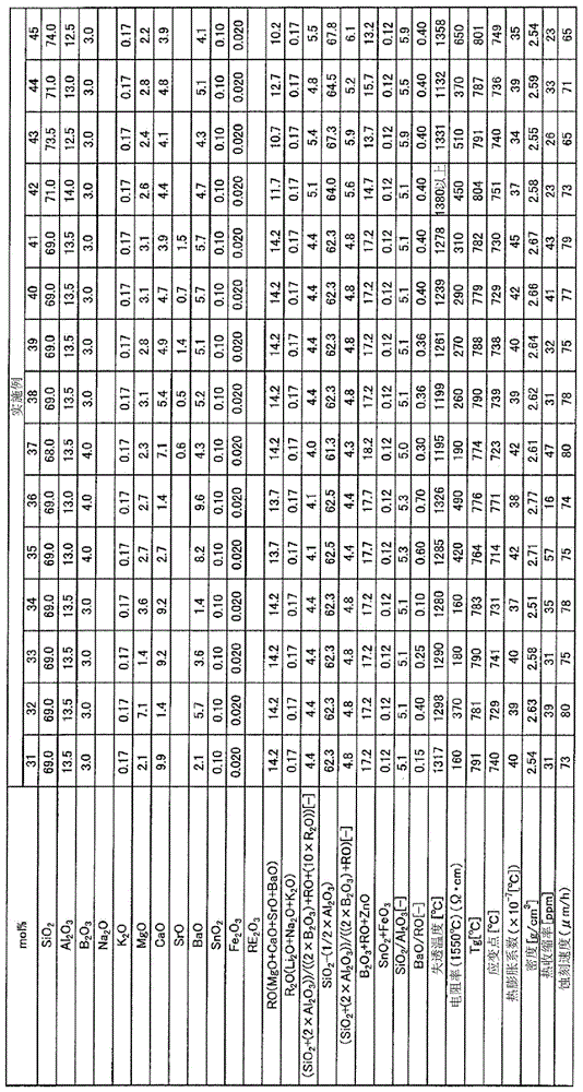
[0352] Hereinafter, this embodiment will be described in more detail based on examples. However, this embodiment is not limited to the Examples. In the following examples and comparative examples, the physical properties described below were measured.

[0353] (strain point)

[0354] The measurement was performed using a beam bending measuring device (manufactured by Tokyo Industrial Co., Ltd.), and the strain point was obtained by calculation in accordance with the beam bending method (ASTMC-598).

[0355] (devitrification temperature)

[0356] The glass was pulverized, and the glass pellets passed through the 2380 μm sieve and remained on the 1000 μm sieve were added to the platinum boat. This platinum boat was held in an electric furnace having a temperature gradient of 1050 to 1380° C. for 5 hours, then taken out from the furnace, and devitrification generated inside the glass was observed with a 50-power optical microscope. The highest temperature at which devitrifica...


PUM

PropertyMeasurementUnit
Resistivityaaaaaaaaaa
Strain pointaaaaaaaaaa

Abstract

The invention relates to a glass substrate for display device and a method for manufacturing same and provides a glass substrate which is high in strain point and capable of preventing a melting tank from melting loss, a glass substrate which is high in strain point and capable of suppressing devitrification, a glass substrate which is high in strain point and etching speed, and a method for manufacturing the glass substrate. The glass substrate contains Sio2 and Al2O3, 0-8% of B2O3, 0.01-0.8 % of R2O, and 0.05-1 of BaO/RO in mol%, and the strain point is over 670 DEG C. The glass substrate may contain Sio2, Al2O3 and MgO, 0.1-0.9 of MgO/(RO+ZnO), the strain point is over 700 DEG C, and the contraction rate is 5ppm-75ppm. The glass substrate may contain Sio2, Al2O3 and BaO, 0-7% of B2O3, 1-15% of BaO, and less than 6.0 of Sio2/Al2O3, and the strain point is over 700 DEG C. RO represents (MgO+CaO+SrO+BaO), and R2O represents (Li2O+Na2O+K2O).

Description

technical field [0001] The invention relates to a glass substrate for a display and a manufacturing method thereof. In particular, the present invention relates to a glass substrate for a low-temperature polysilicon thin film transistor (hereinafter, referred to as LTPS-TFT (Low-Temperature-Polycrystalline-Silicon Thin-Film-Transistor)) display. Also, the present invention relates to a glass substrate for an oxide semiconductor thin-film transistor (hereinafter referred to as OS-TFT (Oxide-Semiconductor Thin-Film-Transistor)) display. More specifically, the present invention relates to a glass substrate for a display in which the above display is a liquid crystal display. Or it relates to a glass substrate for a display in which the display is an organic EL display. Moreover, this invention relates to the glass substrate for flat panel displays in which the said display is a flat panel display. Background technique [0002] LTPS is expected to be used in the manufacture o...

Claims


Application Information

Patent Timeline
IPC IPC(8): C03C3/083C03C3/085C03C3/087C03C3/091
CPCY02P40/57
Inventor 市川学小山昭浩
Owner AVANSTRATE INC
Why Eureka
Try Eureka