Pattern forming method

A pattern and extension direction technology, applied in the field of pattern formation, can solve problems such as line edge distortion of patterns, and achieve uniform arrangement density, improved precision, and good performance.

Active Publication Date: 2014-07-09
SEMICON MFG INT (SHANGHAI) CORP
View PDF4 Cites 8 Cited by
  • Summary
  • Abstract
  • Description
  • Claims
  • Application Information

AI Technical Summary

Problems solved by technology

[0012] However, as the process node of semiconductor technology continues to decrease, especially when the semiconductor process node moves from 32nm to 20nm or even lower, the edge of the patterned line obtained by using the existing SADP technology is distorted.

Method used


Image

  • Pattern forming method
  • Pattern forming method
  • Pattern forming method

Examples


Embodiment Construction

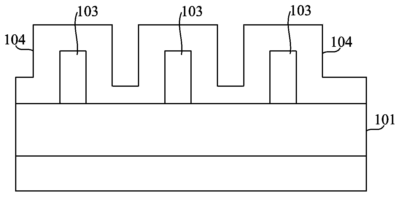
[0054] The inventor has conducted research on the problems existing in the SADP technology of the prior art, and found that: first, refer to Figure 5 and Figure 4, use the sidewall 105 as a mask to etch and remove the sacrificial line 103. In this process, after the sacrificial line 103 is removed, the surface of the sidewall 105 in contact with the sacrificial line 103 has a concave-convex or jagged shape, and the line width roughness (Line Width Roughness, LWR) is higher. If the surface of the sidewall 105 has a concave-convex or jagged shape, when the sidewall 105 is used as a mask to etch the film layer 101 to form the line 106, the concave-convex or zigzag shape of the sidewall 105 in the direction of the extension of the sacrificial line is reflected in the The sidewalls of the wires 106 make the sidewalls of the wires 106 have a concave-convex shape or a zigzag shape. Then, the hole pitch of the pattern including the lines 106 with concave-convex or serrated sidewal...


PUM


Abstract

A pattern forming method comprises the steps that a film layer and an etching barrier layer placed on the film layer are formed on a substrate; a plurality of first patterns, which are arrayed in parallel at equal intervals, of a first line are formed on the etching barrier layer; a second line is formed on the side wall of the first line, wherein the line width of the second line is equal to the line width of the first line, and the second line is made of materials different from that of the first line; a third line is formed in the side wall of the second line, and the line width of the third line is equal to the line width of the first line; a fourth line is arranged on the side wall of the third line in an epitaxial growth mode, the line width of the fourth line is equal to the line width of the first line, and the fourth line is made of materials different from that of the third line; the parts, which are not covered with the first line, the second line, the third line and the fourth line, of the etching barrier layer are removed to expose the film layer; a fifth line is arranged on the film layer in an epitaxial growth mode, and the fifth line is made of materials different from that of the fourth line; the second line and the fourth line are removed, and the patterns which are finally formed comprise the first line, the second line and the fifth line. The patterns have even array density and a good line width, and therefore a semiconductor device formed by the patterns is good in performance.

Description

technical field [0001] The invention relates to the technical field of semiconductors, in particular to a pattern forming method. Background technique [0002] In the field of semiconductor technology, in order to improve the performance of semiconductor devices and reduce production costs, the integration level of integrated circuits is getting higher and higher, and the feature size of transistors on integrated circuits is getting smaller and smaller. Accordingly, in specific production, it is necessary to provide more precise technology to form finer patterns on the semiconductor substrate. [0003] In the prior art, photolithography technology can define and form patterns of semiconductor devices on a substrate, and has been widely used. However, as the semiconductor process node enters 65 nanometers, 45 nanometers, and even lower 32 nanometers, when the characteristic size of the exposed lines in lithography technology is close to the theoretical resolution limit of th...

Claims


Application Information

Patent Timeline
IPC IPC(8): H01L21/3105
CPCH01L21/76886
Inventor 王新鹏
Owner SEMICON MFG INT (SHANGHAI) CORP
Why Eureka
Try Eureka