Small-area high-linearity shaping circuit

A technology for forming circuits and high linearity, applied in electrical components, power oscillators, etc., can solve problems such as poor linearity, achieve the effect of reducing chip area, ensuring constant gain, and improving linearity

Active Publication Date: 2017-01-25
NORTHWESTERN POLYTECHNICAL UNIV
View PDF5 Cites 0 Cited by
  • Summary
  • Abstract
  • Description
  • Claims
  • Application Information

AI Technical Summary

Problems solved by technology

[0007] In order to overcome the deficiency of poor linearity of existing shaping circuits, the present invention provides a shaping circuit with small area and high linearity

Method used


Image

  • Small-area high-linearity shaping circuit
  • Small-area high-linearity shaping circuit
  • Small-area high-linearity shaping circuit

Examples


Embodiment Construction

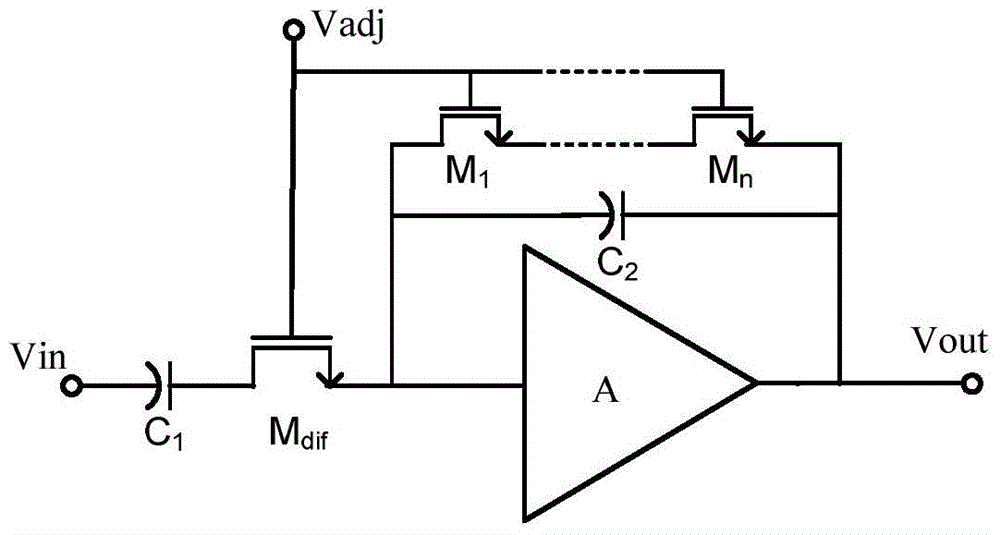
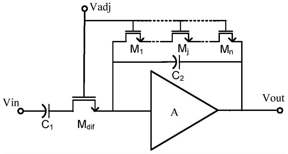
[0018] The following examples refer to Figure 1-2 .

[0019] The small-area high-linearity forming circuit of the present invention includes a capacitor C 1 , capacitance C 2 and operational amplifier A, also includes an NMOS transistor M dif and n NMOS transistors M 1 ~ M n . Capacitance C 1 One end of the forming circuit is connected to the input terminal Vin, and the capacitor C 1 The other end of the NMOS transistor M dif The drain of the NMOS transistor M dif The sources of are respectively connected to the input terminal of the operational amplifier A, n NMOS transistors M 1 ~ M n Drain and capacitance C after series connection 2 one end. The output terminal of the operational amplifier A, n NMOS transistors M 1 ~ M n The source and capacitor C after series connection 2 The other end is connected to the output end Vout of the shaping circuit. NMOS transistor M dif and NMOS transistor M 1 ~ M n The gates of are connected to the time adjustment control ...


PUM


Abstract

The invention discloses a small-area high-linearity shaping circuit which is used for solving the technical problem that an existing shaping circuit is poor in linearity. According to the technical scheme, the small-area high-linearity shaping circuit comprises a capacity C1, a capacity C2, an operational amplifier A, a NMOS transistor Mdif and n NMOS transistors (M1-Mn). A series-connection RC network is formed by the capacitor C1 and the NMOS transistor Mdif. A parallel-connection RC network is formed by the capacitor C2 and the n NMOS transistors (M1-Mn). Due to the fact that a large-resistance resistor of the circuit is obtained through the NMOS transistors, the chip area is greatly reduced. Due to the fact that the large-resistance resistor is obtained by connecting the NMOS transistors in series, the influence of the voltage of source electrodes and drain electrodes of the transistors on the whole resistance value is reduced, and the linearity is improved. When the shaping time is adjusted, the derivative time and the integral time are adjusted at the same time, and it is ensured that the gain of the shaping circuit is unchanged.

Description

technical field [0001] The invention relates to a shaping circuit, in particular to a shaping circuit with small area and high linearity. Background technique [0002] refer to image 3 . Document 1 "Nuclear Electronics (on), 1983, pp.182" discloses a CR-RC forming circuit. The shaping circuit consists of an operational amplifier A, a series CR network (capacitor C 1 and resistor R 1 ) and a parallel RC network (resistor R 2 and capacitance C 2 ). Capacitance C 1 and resistor R 1 form a differential circuit, the capacitor C 2 and resistor R 2 form an integrating circuit. Operational amplifier A isolates these two resistor networks from the circuitry preceding and following the shaping circuit. When the resistance and capacitance products of the differential circuit and the integration circuit are equal, that is, R 1 C 1 =R 2 C 2 =τ, the shaping time of the output waveform of the shaping circuit is about τ. In this way, the forming time can be changed by adjus...

Claims


Application Information

Patent Timeline
Patent Type & Authority Patents(China)
IPC IPC(8): H03B5/12
Inventor 王佳高德远魏廷存高武郑然魏晓敏胡永才
Owner NORTHWESTERN POLYTECHNICAL UNIV
Why Eureka
Try Eureka