Single crystal silicon loading system

A single crystal silicon and power system technology, applied in the direction of conveyor objects, furnaces, lighting and heating equipment, etc., to achieve the effect of improving production efficiency and reducing production costs

Inactive Publication Date: 2014-07-16
SIP GOLDWAY TECH
View PDF8 Cites 3 Cited by
  • Summary
  • Abstract
  • Description
  • Claims
  • Application Information

AI Technical Summary

Problems solved by technology

[0003] In view of the above problems, it is necessary to provide a single crystal silicon feeding system to solve the problem of automatic feeding of single crystal silicon

Method used


Image

  • Single crystal silicon loading system
  • Single crystal silicon loading system
  • Single crystal silicon loading system

Examples


Embodiment Construction

[0035] In order to make the object, technical solution and advantages of the present invention clearer, the present invention will be described in detail below in conjunction with the accompanying drawings and specific embodiments.

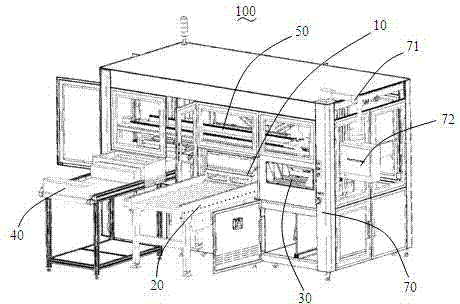
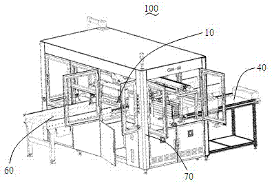
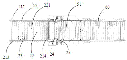
[0036] When manufacturing silicon wafers, it is necessary to sequentially bond the silicon crystal fixtures, resin, and single crystal silicon used to fix the single crystal silicon with glue. see figure 1 and combine figure 2 As shown, the monocrystalline silicon bonding machine 100 of the present invention realizes the automation of the bonding of crystal silicon fixtures, resin and monocrystalline silicon. The monocrystalline silicon bonding machine 100 includes a fixing fixture 10 for fixing the crystalline silicon fixture, a crystalline silicon fixture feeding system 20, a resin feeding system 30, a monocrystalline silicon feeding system 40, and the crystalline silicon fixture. The operating system 50 connected to the feeding system 20 and...


PUM


Abstract

The invention discloses a single crystal silicon loading system. The single crystal silicon loading system comprises a support, a transport portion installed on the support, a correction portion which is installed on the support and stretches across the transport portion, a power system which provides power for the transport portion, and a position sensor installed at one end of the support and used to sense whether the transport portion is provided with single crystal silicon or not. Compared with the prior art, the single crystal silicon loading system achieves the result that the single crystal silicon can be automatically loaded when silicon slices are automatically produced on a large scale, and therefore the single crystal silicon loading system facilitates production efficiency improvement of the silicon slices and production cost reduction of the silicon slices.

Description

technical field [0001] The invention relates to a single crystal silicon feeding system, in particular to a single crystal silicon feeding system for a single crystal silicon bonding machine for realizing automatic bonding of single crystal silicon. Background technique [0002] When manufacturing silicon wafers, it is necessary to sequentially bond the silicon crystal fixtures, resin, and single crystal silicon used to fix the single crystal silicon with glue. At present, in China, the bonding of the crystal silicon fixture, resin and single crystal silicon is done manually. This makes the production efficiency of the silicon wafer relatively low and the production cost high, which is not conducive to realizing the large-scale production of the silicon wafer. In order to realize the large-scale automatic production of silicon wafers, the problem of automatic feeding of monocrystalline silicon must be solved. [0003] In view of the above problems, it is necessary to provi...

Claims


Application Information

Patent Timeline
Patent Type & Authority Applications(China)
IPC IPC(8): B65G47/04B65G49/07
Inventor 李佳
Owner SIP GOLDWAY TECH
Why Eureka
Try Eureka