A reverse conduction double gate insulated gate bipolar transistor

A bipolar transistor, gate insulation technology, applied in semiconductor devices, electrical components, circuits, etc., can solve problems such as unfavorable practical application of LIGBT devices, excessive device current density, current rebound and other problems, and reduce the forward conduction voltage. The effect of reducing, improving current capability, and reducing turn-off loss

Active Publication Date: 2016-08-31
SOUTHEAST UNIV
View PDF4 Cites 0 Cited by
  • Summary
  • Abstract
  • Description
  • Claims
  • Application Information

AI Technical Summary

Problems solved by technology

But it also has a very serious current rebound phenomenon
When multiple LIGBT devices are connected in parallel, if there is a phenomenon of current bounce in the device, it will cause the current density of a single device to be too high and burn out, which is not conducive to the practical application of LIGBT devices

Method used


Image

  • A reverse conduction double gate insulated gate bipolar transistor
  • A reverse conduction double gate insulated gate bipolar transistor
  • A reverse conduction double gate insulated gate bipolar transistor

Examples


Embodiment Construction

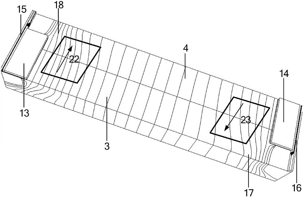
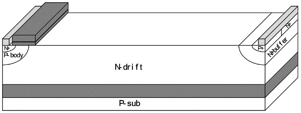
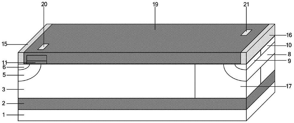
[0027] Combine below figure 2 , to describe the present invention in detail, a reverse conduction type double gate insulated gate bipolar transistor, comprising: a reverse conduction type double gate insulated gate bipolar transistor, comprising: a P-type substrate 1 and a field oxide layer 19, A buried oxygen 2 is provided on the P-type substrate 1, and a drift region is provided on the buried oxygen 2. It is characterized in that the drift region includes a first N-type drift region 3, a first P-type drift region 4, a second The N-type drift region 17 and the second P-type drift region 18, the first N-type drift region 3 and the first P-type drift region 4 are arranged diagonally, the second N-type drift region 17 and the second P-type drift region Zone 18 diagonally set,

[0028] A P-type body region 5 is provided in the first N-type drift region 3 and the second P-type drift region 18, and a heavily doped N-type emitter region 6 and a heavily doped P-type region 5 are ar...


PUM


Abstract

The invention provides a semiconductor capable of improving the current rebounding phenomenon of a reverse-conducting double-insulated-gate bipolar transistor, improving the turn-off speed and improving voltage resistance. The semiconductor is structurally characterized in that a buried oxide is arranged on a P-type substrate and provided with a drift region, the drift region comprises a first N-type drift region, a first P-type drift region, a second N-type drift region and a second P-type drift region, the first N-type drift region and the first P-type drift region are arranged in an opposite-angle mode, and the second N-type drift region and the second P-type drift region are arranged in an opposite-angle mode; a P-type region is arranged in the first N-type drift region and the second P-type drift region, an N-type emitter region, a P-type collector region and cathode metal connecting the N-type emitter region with the P-type collector region are arranged in the P-type region, and a cathode gate oxide and a cathode polycrystalline silicon layer are arranged on the upper surface of the P-type region; an N-type region is arranged in the first P-type drift region and the second N-type drift region, an N-type collector region, a P-type emitter region and anode metal connecting the N-type collector region with the P-type emitter region are arranged in the N-type region, and an anode gate oxide and an anode polycrystalline silicon layer are arranged on the upper surface of the N-type region.

Description

technical field [0001] The present invention mainly relates to the technical field of power semiconductor devices, specifically, it is a reverse conduction double-gate insulated gate bipolar transistor, which is especially suitable for high-power integrated circuits such as frequency conversion speed regulation, electric traction, frequency conversion household appliances, and half-bridge drives. Circuits and automobile production and other fields. Background technique [0002] Insulated gate bipolar transistor IGBT is a composite power device evolved from the combination of MOS gate device structure and bipolar transistor structure. It has the characteristics of both MOS transistor and bipolar transistor, and has good on-state current and switching [0003] The trade-off relationship between losses. Silicon-on-insulator lateral insulated gate bipolar transistor (SOI-Lateral Insulated Gate Bipolar Transistor, SOI-LIGBT) is a typical device based on SOI technology, which has...

Claims


Application Information

Patent Timeline
Patent Type & Authority Patents(China)
IPC IPC(8): H01L29/739H01L29/06H01L29/423
CPCH01L29/0619H01L29/423H01L29/7393
Inventor 孙伟锋杜益成杨卓祝靖徐申陆生礼时龙兴
Owner SOUTHEAST UNIV
Why Eureka
Try Eureka