Double-gate SOI-LIGBT device with P-type buried layer

A device, N-type technology, applied in the direction of semiconductor devices, electrical components, circuits, etc., can solve the problems of increasing the current capacity of the device, and no good solution has appeared, to increase the current capacity, reduce the size, and reduce the on-resistance. Effect

Inactive Publication Date: 2013-09-25
SICHUAN CHANGHONG ELECTRIC CO LTD
View PDF5 Cites 5 Cited by
  • Summary
  • Abstract
  • Description
  • Claims
  • Application Information

AI Technical Summary

Problems solved by technology

[0005] In order to achieve high integration of the chip, it is a good solution to further reduce the area of ​​the chip and minimize the size of the SOI-LIGBT device in the width direction. However, at present, it is necessary to further reduce the device under the condition of ensuring its withstand voltage The size in the width direction can only be achieved by increasing the current capability of the device, and there is no good solution yet.

Method used


Image

  • Double-gate SOI-LIGBT device with P-type buried layer
  • Double-gate SOI-LIGBT device with P-type buried layer

Examples


Embodiment Construction

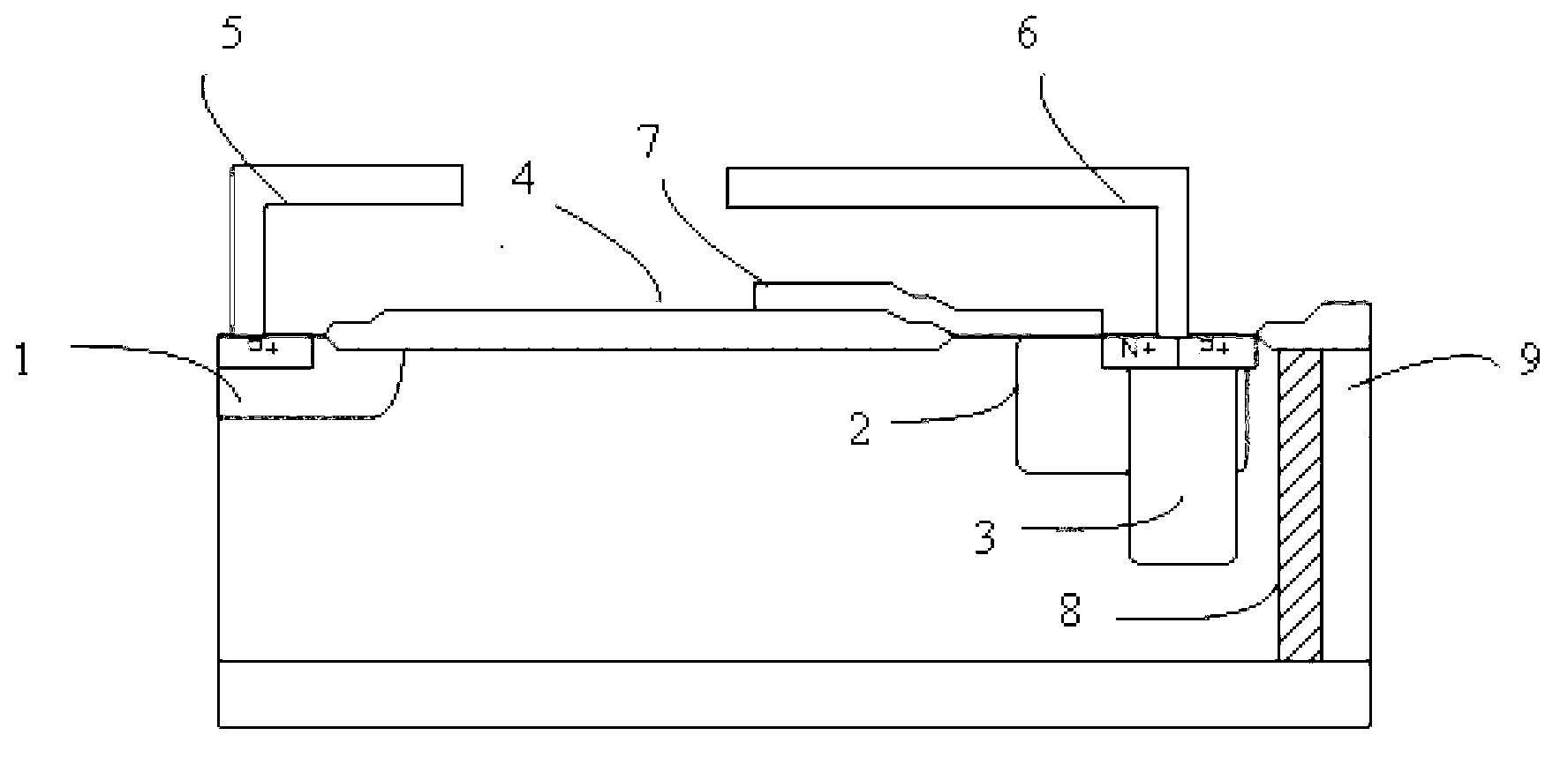
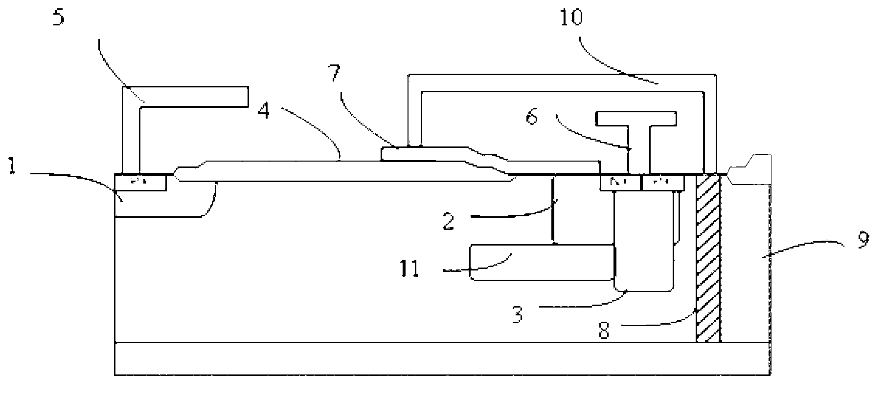
[0013] The traditional LIGBT device introduces RESURF technology, and its source, drain, and gate field plates smooth the high electric field peaks formed at the surface field oxygen and drift regions of the device, making the electric field closer to the rectangular distribution and achieving higher resistance. However, in the on-state process, the current line mainly flows from the surface of the device, and the current in the body area is small, causing a certain waste; in response to this problem, the present invention proposes a new type of SOI-LIGBT device, by increasing P-type buried layer, and the filling material in the isolation trench is converted from traditional bulk silicon to filled polysilicon, and the isolation trench is connected to the gate terminal electrode through a metal structure, thereby using it as a gate electrode in the side direction of the device, making it It can be used as a gate field plate to reduce the electric field near the channel region to ...


PUM


Abstract

The invention relates to a semiconductor device and discloses a double-gate SOI-LIGBT device with a P-type buried layer. Under the condition that voltage resistance is ensured, the current capacity of the device is enhanced. According to the double-gate SOI-LIGBT device, the P-type buried layer is additionally arranged, traditional bulk silicon is changed into polycrystalline silicon for serving as filling materials of a separation groove, the separation groove is connected with a gate end electrode through a metal structure and accordingly serves as a gate electrode in the lateral direction of the device. The double-gate SOI-LIGBT device not only can serve as a gate field plate to be shrunk into an electric field near a channel region for meeting the voltage resistance requirement. Meanwhile, the double-gate SOI-LIGBT device can serve as a longitudinal gate electrode so that the current can stream on the surface and can also stream below the P-type buried layer in a device body area, the current capacity is enhanced, on-resistance is reduced, and therefore the size of the device in the width direction can be shortened under the condition that the voltage resistance is ensured. The double-gate SOI-LIGBT device with the P-type buried layer is suitable for a PDP scanning driving chip.

Description

Technical field [0001] The invention relates to a semiconductor device, in particular to a novel dual-gate SOI-LIGBT (Silicon-on-Insulator-Horizontal Insulated Gate Transistor) device with a P-type buried layer used in a PDP scan drive chip. Background technique [0002] Plasma displays have been widely used due to their wide color gamut and fast dynamic response. Among them, the line scan driver chip is used for the horizontal line scan of the display and is a key component of the plasma display. In the design of the line scan driver chip, it is necessary to output 96 channels of independent high voltage. The output stage includes a pull-up transistor and a pull-down transistor. The current capability of the pull-down transistor needs to reach 1.5A and the off-state withstand voltage is 200V, so the width of the transistor is relatively large, 96 channels The total area of ​​the pull-down LIGBT (lateral insulated gate transistor) reaches 30% of the overall chip area. [0003] Th...

Claims


Application Information

Patent Timeline
Patent Type & Authority Applications(China)
IPC IPC(8): H01L29/739H01L29/40H01L29/423
Inventor 孙镇黄勇
Owner SICHUAN CHANGHONG ELECTRIC CO LTD
Why Eureka
Try Eureka