Electrostatic discharging protection circuit triggered by lining-bottom

An electrostatic discharge protection and substrate technology, which is applied to circuits, electrical components, and electrical solid devices, etc., and can solve problems such as uneven opening and large bulk resistance.

Inactive Publication Date: 2007-06-13
SHANGHAI HUA HONG NEC ELECTRONICS
View PDF0 Cites 5 Cited by
  • Summary
  • Abstract
  • Description
  • Claims
  • Application Information

AI Technical Summary

Problems solved by technology

In this form, when ESD occurs, due to the difference in the bulk resistance of the transistor to the well control (guard-ring) at different positions, it will lead to uneven opening, as shown in Figure 3. In the middle part of the device, due to its off-well control ) the farthest, the largest body resistance, the easiest to turn on before other finger (Finger) devices

Method used


Image

  • Electrostatic discharging protection circuit triggered by lining-bottom
  • Electrostatic discharging protection circuit triggered by lining-bottom

Examples


Embodiment Construction

[0010] The present invention will be described in further detail below in conjunction with the accompanying drawings.

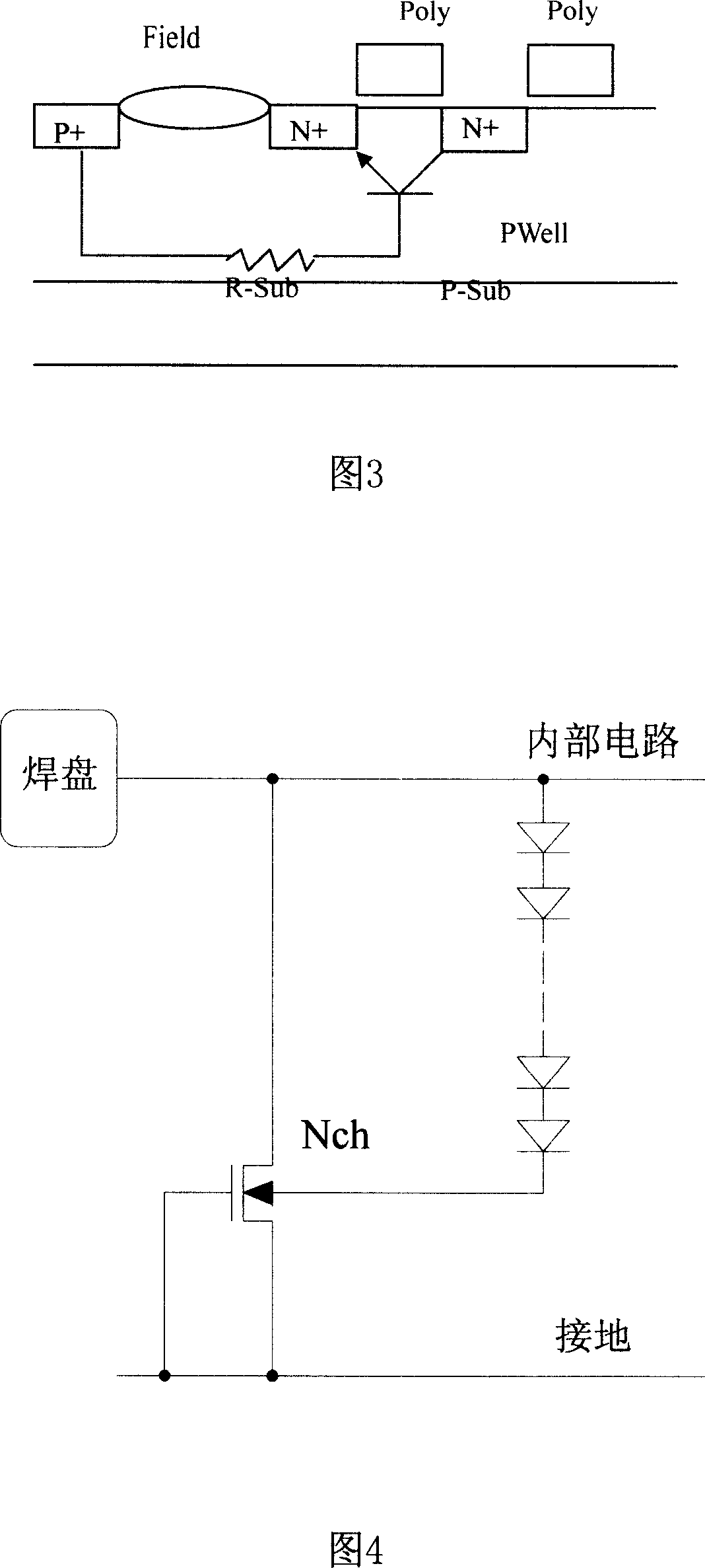
[0011] The circuit provided by the present invention is shown in Figure 4. In the traditional structure using GGNMOS as an ESD protection circuit, a voltage-dividing diode string is added, and the anodes and cathodes of every two adjacent diodes in the diode string are connected end to end. The diode string is placed between the previous stage of the internal circuit and the N-type metal oxide buffer (Nch Buffer) transistor substrate (bulk), the anode of the first diode is connected to the previous stage of the internal circuit, and the cathode of the tail diode is connected to the Nch Buffer The substrates of the transistors are connected, and the number of stages of the diode string is designed to make its turn-on voltage larger than the normal voltage operating range, but slightly smaller than the breakdown voltage of the Nch Buffer transistor. If the norm...


PUM


Abstract

The protection circuit includes N type metallic oxide buffer (Nch Buffer) transistor, and a diode string. Grid of (Nch Buffer) transistor is connected to ground. Substrate is connected to cathode of diode at tail of the diode string. Anode of diode at header of the diode string is connected to previous stage of the internal circuit. When static discharge occurs, before Nch Buffer transistor turns on, the diode string generates current, which provides substrate current for Nch Buffer transistor, and generates substrate bias voltage so as to trigger Nch Buffer transistor. When static discharge occurs, the invention triggers and turns transistor to on quicker, provides larger current release capability, and turns transistor to on uniformly.

Description

technical field [0001] The invention relates to an electrostatic discharge protection circuit, in particular to an electrostatic discharge protection circuit using a diode string. Background technique [0002] Integrated circuits are easily damaged by electrostatic discharge (ESD). Generally, an electrostatic protection circuit is designed in the input and output terminals of the circuit or power supply protection to prevent internal circuits from being damaged. The gate grounding N-channel metal oxide semiconductor (GGNMOS) is A widely used protective structure is shown in Figure 1. In order to ensure a certain protection strength, GGNMOS is generally in the form of multi-finger parallel connection, as shown in Figure 2. In this form, when ESD occurs, due to the difference in the bulk resistance of the transistor to the well control (guard-ring) at different positions, it will lead to uneven opening, as shown in Figure 3. In the middle part of the device, due to its off-we...

Claims


Application Information

Patent Timeline
Patent Type & Authority Applications(China)
IPC IPC(8): H01L23/60
Inventor 徐向明
Owner SHANGHAI HUA HONG NEC ELECTRONICS
Why Eureka
Try Eureka