Method for subsection integral of silicon array detector

A detector and silicon array technology, applied in the field of photoelectric detection, can solve problems such as output signal saturation, achieve the effects of low cost, high reliability, and avoid complex design

Active Publication Date: 2014-08-06
CHANGCHUN INST OF OPTICS FINE MECHANICS & PHYSICS CHINESE ACAD OF SCI
View PDF5 Cites 2 Cited by
  • Summary
  • Abstract
  • Description
  • Claims
  • Application Information

AI Technical Summary

Problems solved by technology

Conversely, the output signal may saturate

Method used


Image

  • Method for subsection integral of silicon array detector
  • Method for subsection integral of silicon array detector
  • Method for subsection integral of silicon array detector

Examples


Embodiment Construction

[0021] Invention idea of ​​the present invention is:

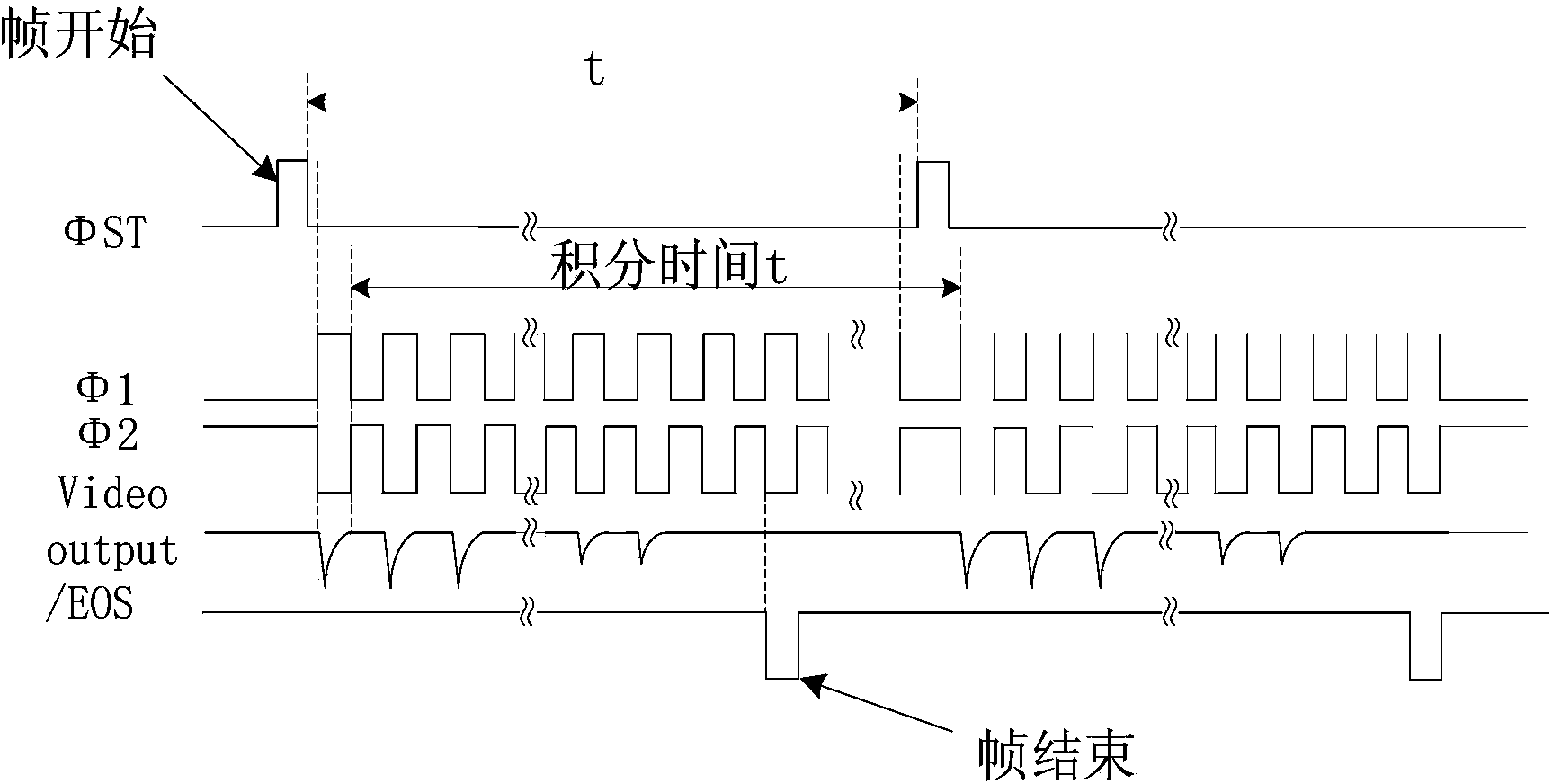
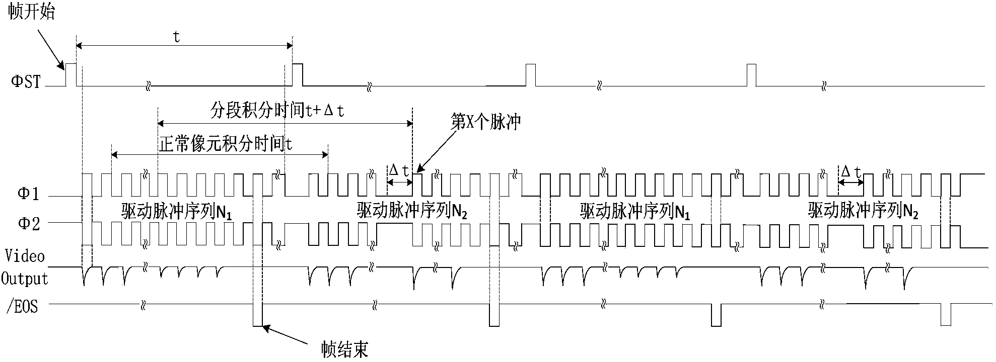
[0022] The so-called segmental integration method is based on the intensity of the light signal incident on the pixels of different segments and the difference in response, by setting the time interval between the driving pulses, to properly adjust the intensity of the pixels in different segments. method of integrating time.

[0023] The silicon array detector segmentation integration method of the present invention changes the clock pulse through software design The time interval is so that the pixels in each section have different integration times, and there is no need to change the external circuit design of the silicon array detector.

[0024] The silicon array detector segmentation integration method of the present invention utilizes the drive pulse sequence N according to the order of the segmentation integration time within a frame 1 and drive pulse sequence N 2 The method of alternating action can gradually...


PUM


Abstract

The invention provides a method for subsection integral of a silicon array detector. A drive pulse timing sequence is changed through software design of a programmable logic array, and therefore the integral time of picture elements of all sections are adjusted. According to the method for the subsection integral of the silicon array detector, the problem that certain picture elements output signals are small due to the fact that incident light of different intensities irradiates on different positions of the silicon array detector is solved, and the signal to noise ratio of the output signals is improved. The subsection integral method is based on software design, is easy to achieve, low in cost and high in reliability, and avoids complex hardware design.

Description

technical field [0001] The invention relates to the technical field of photoelectric detection, and provides a method for segmental integration of a silicon array detector. Background technique [0002] The silicon array detector is a self-scanning photodiode array device designed for multi-channel spectral imaging detection. When the incident light from the imaging target and through the optical system hits the silicon array detector, under the control of the clock pulse and the start pulse, the charge signal generated by the detector is read out from the signal output line. The output charge of the silicon array detector is equal to the product of the illuminance of the incident light, the integration time and the spectral sensitivity. The time interval between two adjacent readout signals corresponding to the same pixel is called the integration time, and this period of time is the accumulation time of photoelectrons generated by the pixel under the irradiation of incide...

Claims


Application Information

Patent Timeline
Patent Type & Authority Applications(China)
IPC IPC(8): G01J3/28
Inventor 宋克非张佩杰武昆
Owner CHANGCHUN INST OF OPTICS FINE MECHANICS & PHYSICS CHINESE ACAD OF SCI
Why Eureka
Try Eureka