
Photoresist removing method

A photoresist and photoresist technology, applied in electrical components, semiconductor/solid-state device manufacturing, circuits, etc., can solve the problem of polluting the internal environment of the reaction chamber, and achieve the effect of purifying the internal environment

Active Publication Date: 2014-08-06
ADVANCED MICRO FAB EQUIP INC CHINA
View PDF8 Cites 4 Cited by
  • Summary
  • Abstract
  • Description
  • Claims
  • Application Information

AI Technical Summary

Problems solved by technology

Since the substrate 504 is in the reaction chamber, the removal figure 2 During the photoresist 112 process, the sputtered silicon particles will not only be deposited on the surface of the photoresist 113, but also the sputtered silicon particles may be deposited on the gas shower head 502, the surface of the lower electrode and the side surface of the reaction chamber. wall 509, thereby forming particles (particles), polluting the internal environment of the reaction chamber to a certain extent

Method used


Image

  • Photoresist removing method
  • Photoresist removing method
  • Photoresist removing method

Examples


Embodiment Construction

[0037]The implementation of the present invention will be described in detail below in conjunction with the drawings and examples, so that the realization process of how to use technical means to solve technical problems and achieve technical effects in the present invention can be fully understood and implemented accordingly.

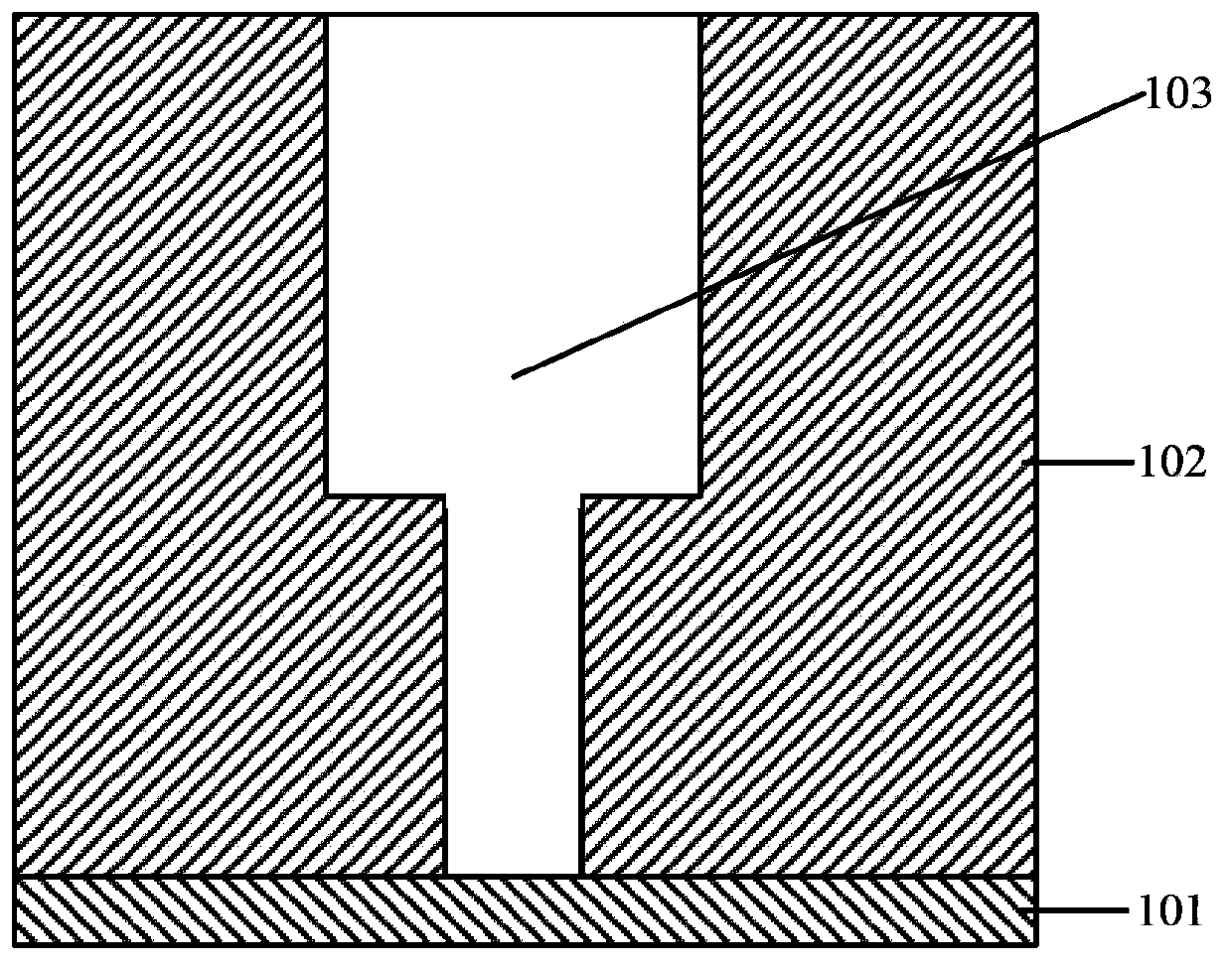
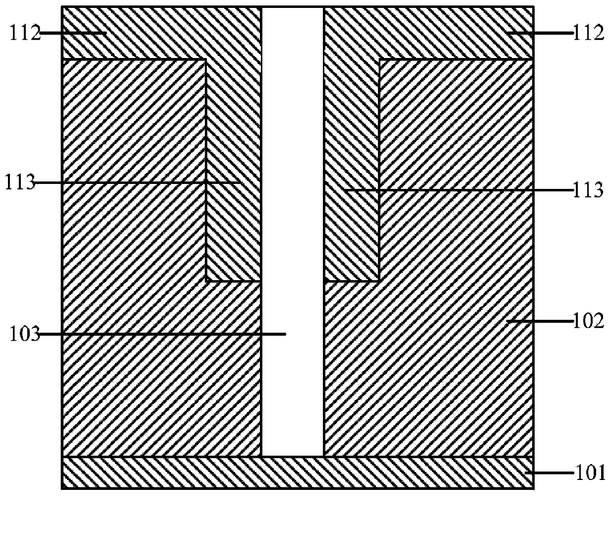
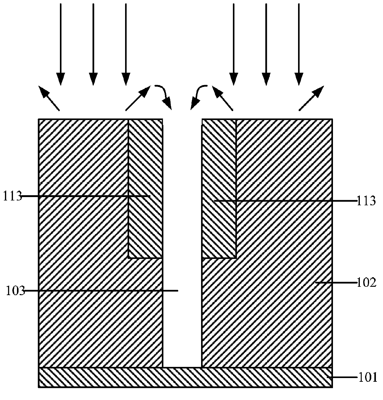
[0038] In the following embodiments of the present invention, during the process of forming the etching opening, in the intermediate step plasma treatment process, while removing part of the photoresist in the sidewall of the etching opening, the photoresist in the previous plasma treatment process is also removed. The sputtered dielectric particles are deposited on the surface of the photoresist, and all the photoresist remaining on the sidewall of the etching opening is removed in the final plasma treatment, so as to complete the removal of the photoresist in the process of etching the opening. In addition, since the dielectric particles sputtered ont...


PUM


Abstract

The invention discloses a photoresist removing method which includes: using a plasma process mainly containing oxygen to remove all the photoresist at the top of a dielectric layer and part of photoresist on the side wall of an etching opening; using a plasma process mainly containing oxygen and F or CL to remove the sputtering dielectric particles of the first step and part of the residual photoresist, after the first step, of the etching opening; using a plasma process mainly containing oxygen to remove all the residual photoresist, after the first step and the second step, of the etching opening. The method has the advantage that during etching opening forming, when part of the photoresist in the etching opening is removed during the intermediate step of plasma processing, the dielectric particles which are sputtered and deposited on the surface of the photoresist during plasma processing are removed at the same time.

Description

technical field [0001] The invention belongs to the technical field of semiconductor manufacturing, and in particular relates to a method for removing photoresist. Background technique [0002] In the semiconductor manufacturing process, it is usually necessary to deposit an electrolyte material and form a photoresist pattern on the surface of the semiconductor device, and then etch the electrolyte material and selectively remove the photoresist formed on the semiconductor surface. [0003] At present, when removing the photoresist on the semiconductor surface, there are usually two methods: dry etching and wet etching. Among them, dry etching refers to the plasma generated by exposing the semiconductor surface to the gaseous state, which has a physical or chemical reaction with the photoresist, thereby removing the photoresist on the semiconductor surface. Dry etching is mostly used in submicron size Device etching. The so-called wet etching is liquid chemical reagents su...

Claims


Application Information

Patent Timeline
Patent Type & Authority Applications(China)
IPC IPC(8): H01L21/027
CPCH01L21/31138
Inventor 王兆祥杜若昕刘骁兵刘志强
Owner ADVANCED MICRO FAB EQUIP INC CHINA
Learn More