Integrated passive device fan-out wafer level packaging structure and manufacturing method

A technology for integrating passive devices and wafer-level packaging, which is applied in semiconductor/solid-state device manufacturing, electric solid-state devices, semiconductor devices, etc., can solve the problems of occupying product assembly costs, shorten the length of electrical connections, and improve the quality factor Q Value, improve the effect of electrical quality

Active Publication Date: 2016-08-24
江苏中科智芯集成科技有限公司
View PDF3 Cites 0 Cited by
  • Summary
  • Abstract
  • Description
  • Claims
  • Application Information

AI Technical Summary

Problems solved by technology

In general, wafer-level fan-out chip packaging does not integrate passive passive devices, and the matching passive devices occupy about 80% of the circuit board area and 70% of the product assembly cost

Method used


Image

  • Integrated passive device fan-out wafer level packaging structure and manufacturing method
  • Integrated passive device fan-out wafer level packaging structure and manufacturing method
  • Integrated passive device fan-out wafer level packaging structure and manufacturing method

Examples


Embodiment Construction

[0028] The present invention will be further described below in conjunction with specific drawings.

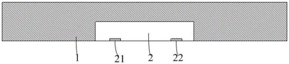
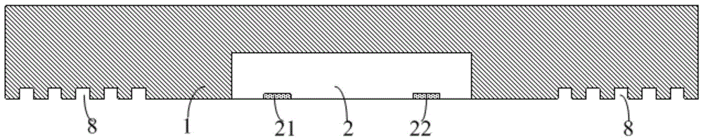
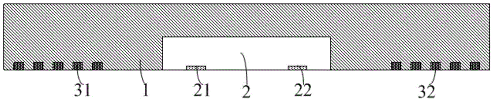
[0029] Such as Picture 10 Shown: the integrated passive device fan-out wafer-level packaging structure includes a molding compound body 1 and a fan-out chip 2 molded in the molding compound body 1. The chip 2 has a first electrode 21 and a second electrode on the front side 22. The front surface of the chip 2 is flush with the front surface of the molding compound body 1; the molding compound body 1 is provided with a first metal wiring layer 31 and a second metal wiring layer 32, a first metal wiring layer 31 and a second metal wiring layer The layer 32 is flush with the front surface of the molding compound body 1; Picture 11 As shown, the first metal wiring layer 31 and the second metal wiring layer 32 are spirally distributed on the molding compound body 1, and electrical characteristics of resistance or inductance are obtained through the spiral structure; on the front sid...


PUM


Abstract

The invention relates to an integrated passive device fan-out-type wafer-level packaging structure and a manufacturing method of the integrated passive device fan-out-type wafer-level packaging structure. The integrated passive device fan-out-type wafer-level packaging structure comprises a modeling plastic body and a chip, and is characterized in that a spiral metal wire distribution layer is arranged in the modeling plastic body, an insulating layer is arranged on the front surface of the modeling plastic body, a metal wire leading layer is distributed in the insulating layer and is connected with an electrode of the chip and the metal wire distribution layer, and a welding ball is arranged on the metal wire leading layer. The manufacturing method of the packaging structure comprises the following steps that (1) the chip is packaged in the modeling plastic body in a plastic mode; (2) a spiral groove body is formed in the front surface of the modeling plastic body, and the metal wire distribution layer is manufactured in the groove body; (3) the insulating layer is manufactured on the front surface of the modeling plastic body, a window is formed in the insulating layer, a metal layer is manufactured on the surface of the insulating layer, a needed graph is etched on the metal layer, and the metal wire leading layer is obtained; (4) an insulating layer is manufactured on the metal wire leading layer, a window is formed in the insulating layer, and the welding ball is manufactured in the window. By means of the integrated passive device fan-out-type wafer-level packaging structure and the manufacturing method of the integrated passive device fan-out-type wafer-level packaging structure, the electric connection length of the chip and a passive device is shortened, and the electric quality is improved.

Description

Technical field [0001] The invention relates to a fan-out wafer-level packaging structure and a manufacturing method of an integrated passive device, belonging to the technical field of fan-out wafer-level packaging. Background technique [0002] Wafer-level fan-out chip packaging can replace the current wire bond BGA (Ball Grid Array, PCB with ball grid array) and flip chip BGA packaging, and is a low-cost, high-performance integrated package. The signal, power and ground wiring of the wafer-level fan-out chip package is directly realized through the wafer-level RDL (rewiring layer) process, which eliminates the need for wafer bump preparation and packaging substrates, thereby reducing packaging costs and Provide better electrical functions than traditional wire bonding BGA and flip chip BGA packages. Thin-film integrated passive technology usually provides the best functional density, as well as the highest integration and the lightest volume. However, from the perspective of...

Claims


Application Information

Patent Timeline
Patent Type & Authority Patents(China)
IPC IPC(8): H01L23/64H01L23/498H01L25/00H01L21/48
CPCH01L24/19H01L2224/12105H01L2224/19H01L2224/24195H01L2924/181H01L2924/00H01L2924/00012
Inventor 孙鹏徐健王宏杰何洪文
Owner 江苏中科智芯集成科技有限公司
Why Eureka
Try Eureka