Chip packaging structure

A chip packaging structure and chip technology, applied in electrical components, electrical solid devices, circuits, etc., can solve the problems of insufficient number of non-signal pads and non-signal pins, large distance between signal pins and non-signal pins, etc. , to achieve the effect of increasing grounding and avoiding noise

Inactive Publication Date: 2014-08-13
ALICORP
View PDF3 Cites 4 Cited by
  • Summary
  • Abstract
  • Description
  • Claims
  • Application Information

AI Technical Summary

Problems solved by technology

[0004] The present invention provides a chip packaging structure to solve the problem of insufficient number of groups of non-signal pads and non-signal pins and the problem of excessive distance between signal pins and non-signal pins

Method used


Image

  • Chip packaging structure
  • Chip packaging structure

Examples


Embodiment Construction

[0034] In order to make the object, technical solution and advantages of the present invention clearer, the embodiments of the present invention will be further described in detail below in conjunction with the accompanying drawings. Here, the exemplary embodiments and descriptions of the present invention are used to explain the present invention, but not to limit the present invention.

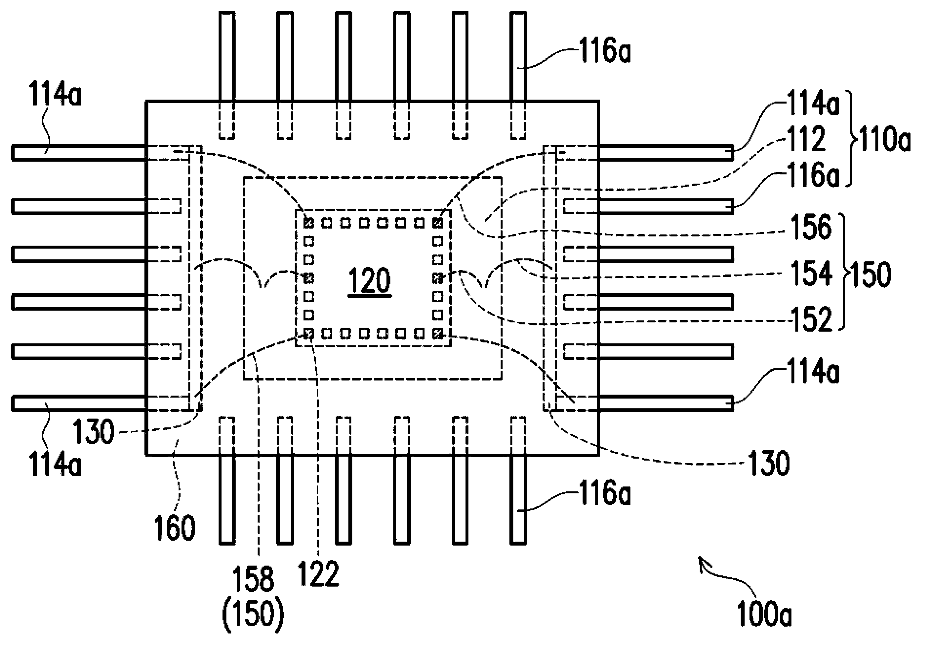
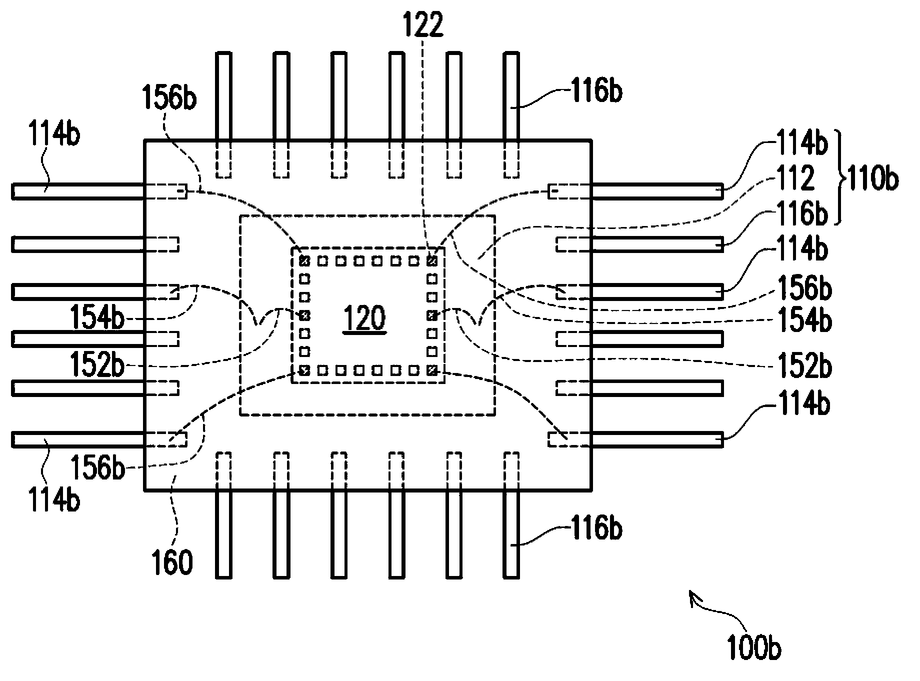
[0035] figure 1 It is a schematic top view of a chip package structure according to an embodiment of the present invention. Please refer to figure 1 , the chip packaging structure 100a of this embodiment includes a lead frame 110a, a chip 120, at least one bus 130 ( figure 1 Two) and a wire group 150 are schematically shown in . In detail, the lead frame 110a includes a chip holder 112, a plurality of ground pins 114a ( figure 1 four) and a plurality of signal pins 116a are schematically shown, wherein the signal pins 116a and the ground pins 114a are arranged around the die holder 112 ....


PUM


Abstract

Disclosed is a chip packaging structure which includes a lead frame, a chip, at least one bus and a lead group. The lead frame includes a chip seat, a plurality of signal pins and a plurality of grounding pins. The signal pins and the grounding pins are arranged around the chip seat. The chip is arranged on the chip seat of the lead frame. The chip is provided with a plurality of grounding bonding pads. The buses are connected with part of the grounding pins of the lead frame. The lead group is connected with the grounding bonding pads of the chip, the signal pins, the grounding pins and the buses.

Description

technical field [0001] The present invention relates to a packaging structure, and in particular to a chip packaging structure. Background technique [0002] The purpose of chip packaging is to provide proper signal path, heat dissipation path and structural protection of the chip. Traditional wire bonding technology usually uses a leadframe as a chip carrier. [0003] Generally speaking, during the wire bonding process, most of the wires are bonded from the signal pins of the lead frame to the I / O pads of the chip. However, when the chip requires more functions, that is, when there are more signal pads with different functions on the chip, the required number of signal pins of the lead frame is relatively increased. Therefore, not only the number of signal pins on the lead frame is likely to be insufficient, but also the signal pads of the chip need to be set in one-to-one correspondence with the signal pins, which limits the position and relationship of non-signal pads. ...

Claims


Application Information

Patent Timeline
Patent Type & Authority Applications(China)
IPC IPC(8): H01L23/495
CPCH01L2924/0002H01L2224/48091H01L2924/19107H01L2224/48247
Inventor 吴信宽黄钲凯
Owner ALICORP
Why Eureka
Try Eureka