Supercharge Your Innovation With Domain-Expert AI Agents!

Array substrate and display panel

A technology of array substrates and data lines, applied in static indicators, nonlinear optics, instruments, etc., can solve the problems of lower product quality, limited discharge speed of storage capacitors, afterimages, etc.

Active Publication Date: 2014-08-20
BOE TECH GRP CO LTD +1
View PDF6 Cites 36 Cited by
  • Summary
  • Abstract
  • Description
  • Claims
  • Application Information

AI Technical Summary

Problems solved by technology

However, with the improvement of the resolution of the display, due to the limited discharge speed of the storage capacitor corresponding to the pixel electrode, there will be afterimage problems in the process of jumping between two frames, which will reduce the product quality.

Method used


Image

  • Array substrate and display panel
  • Array substrate and display panel
  • Array substrate and display panel

Examples


Embodiment approach

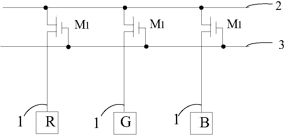
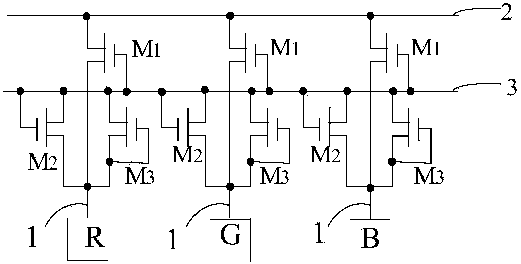
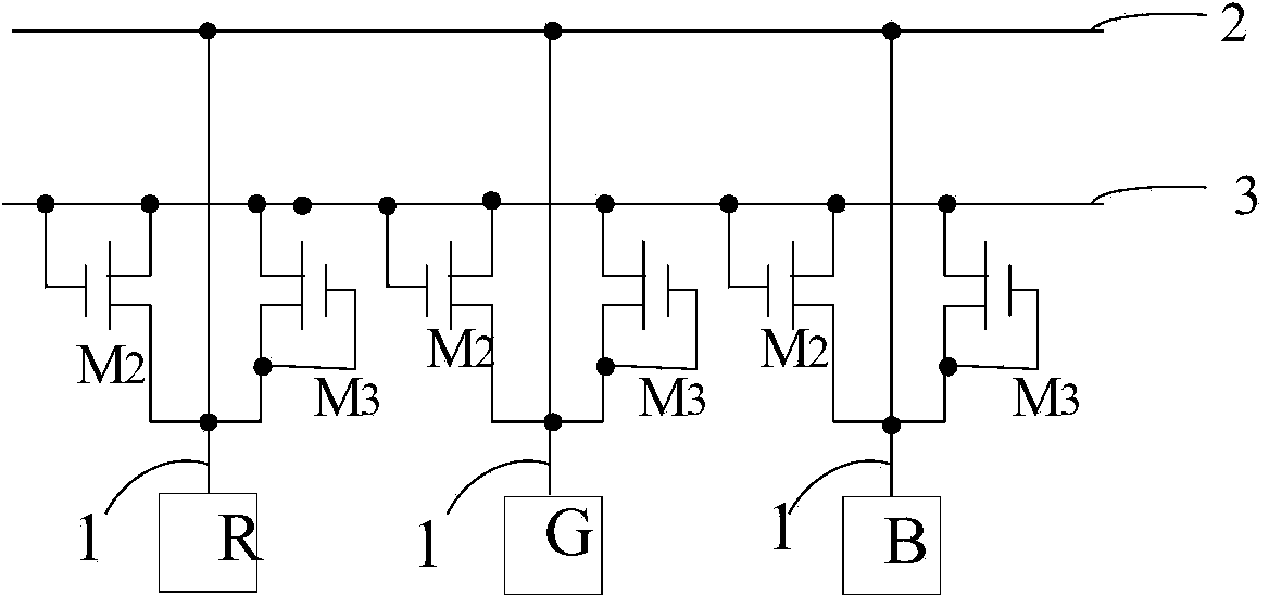
[0038] As a specific embodiment of the present invention, the array substrate may further include a driving circuit, such as figure 1 and figure 2 As shown, the discharge unit includes a first thin film transistor M 1 , the first thin film transistor M 1 The gate of the gate is connected to the output terminal of the driving circuit, and the first thin film transistor M 1One of the source and the drain is connected to the data line 1, and the other is connected to the common electrode line 2. The driving circuit can output a control signal between displaying two frames of images, so that the first thin film transistor M1 is turned on, so as to turn on the data line and the common electrode line connected to the first thin film transistor M1.

[0039] In the present invention, the first thin film transistor M 1 The gate of the gate can be directly connected to the driving circuit, and can also be indirectly connected to the driving circuit. As a preferred embodiment of th...


PUM


Abstract

The invention provides an array substrate which comprises a plurality of data lines and a plurality of public electrode lines. The array substrate further comprises a discharging unit, the discharging unit is arranged between at least one data line and at least one public electrode line, and the data line connected with the discharging unit can be selectively communicated with the public electrode line connected with the discharging unit through the discharging unit. The invention further provides a display panel of the array substrate. According to the array substrate and the display panel, the data line connected with the discharging unit can be selectively communicated with the public electrode line connected with the discharging unit through the discharging unit, a storage capacitor can accordingly and rapidly conduct discharging, and incidental images are reduced.

Description

technical field [0001] The invention relates to the technical field of liquid crystal display, in particular to an array substrate and a display panel. Background technique [0002] Thin film transistor display (TFT-LCD) has been widely used due to its advantages of high image quality, low power and low cost after several decades of development. [0003] During the working process of the liquid crystal display, when the liquid crystal display is displaying images, the thin film transistor corresponding to the pixel electrode is turned on, and the signal can be transmitted to the pixel electrode through the data line, which is to charge the storage capacitor formed by the pixel electrode and the common electrode. When the liquid crystal display does not display an image (that is, when displaying two frames of pictures), the storage capacitor formed by the pixel electrode and the common electrode is discharged. However, with the improvement of display resolution, due to the l...

Claims


Application Information

Patent Timeline
Patent Type & Authority Applications(China)
IPC IPC(8): G02F1/1362G02F1/1368
CPCG02F1/136204G02F1/136286G02F1/136254G09G3/3648G09G2300/0404G09G2300/0426G09G2300/0478
Inventor 魏向东郝学光李成安星俊柳奉烈
Owner BOE TECH GRP CO LTD
Features
  • R&D
  • Intellectual Property
  • Life Sciences
  • Materials
  • Tech Scout
  • Unparalleled Data Quality
  • Higher Quality Content
  • 60% Fewer Hallucinations
Learn More