Method for Improving the Uniformity of Resistivity of Epitaxial Layer

An epitaxial layer and resistivity technology, applied in chemical instruments and methods, circuits, electrical components, etc., can solve the problems of poor uniformity of resistivity of epitaxial layers, improve the uniformity of resistivity, reduce the influence of uniformity of resistivity, The effect of improving product yield

Active Publication Date: 2016-07-06
ADVANCED SEMICON MFG CO LTD
View PDF4 Cites 0 Cited by
  • Summary
  • Abstract
  • Description
  • Claims
  • Application Information

AI Technical Summary

Problems solved by technology

[0005] The object of the present invention is to provide a method for improving the uniformity of the resistivity of the epitaxial layer to solve the problem of poor uniformity of the resistivity of the epitaxial layer on the substrate caused by the self-doping phenomenon

Method used


Image

  • Method for Improving the Uniformity of Resistivity of Epitaxial Layer

Examples


Embodiment Construction

[0022] The method for improving the resistivity uniformity of the epitaxial layer proposed by the present invention and the manufacturing method thereof will be further described in detail below with reference to the accompanying drawings and specific embodiments. Advantages and features of the present invention will be apparent from the following description and claims. It should be noted that all the drawings are in a very simplified form and use imprecise scales, and are only used to facilitate and clearly assist the purpose of illustrating the embodiments of the present invention.

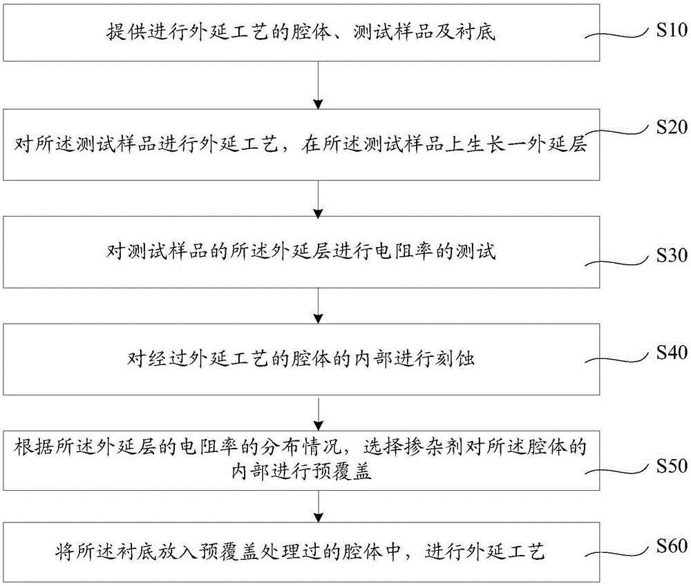
[0023] Please refer to figure 1 , which is a flowchart of a method for improving resistivity uniformity of an epitaxial layer according to an embodiment of the present invention. Such as figure 1 As shown, the method for improving the uniformity of the resistivity of the epitaxial layer comprises the following steps:

[0024] Firstly, step S10 is performed to provide a cavity for epitaxial p...


PUM


Abstract

The invention provides a method for improving the uniformity of the electrical resistivity of an epitaxial layer. According to the method for improving the uniformity of the electrical resistivity of the epitaxial layer, pre-covering is conducted inside a cavity with a selected dopant according to the distribution condition of the electrical resistivity of the epitaxial layer grown on a test sample, namely, a film containing the dopant is grown inside the cavity, and then epitaxy processing is conducted on a substrate. In the epitaxy process, the dopant on the internal side wall of the pre-covered cavity and a base can be diffused out under the influence of high temperature, and thus the concentration of the dopant gas on the edge of the substrate can be changed; the dopant gas enters the epitaxial layer, the distribution of the electrical resistivity of the epitaxial layer is changed, the influence of doping on the uniformity of the electrical resistivity of the epitaxial layer is reduced, and the qualified rate of products is increased.

Description

technical field [0001] The invention relates to the technical field of semiconductor manufacturing, in particular to a method for improving the resistivity uniformity of an epitaxial layer. Background technique [0002] The epitaxial process refers to the growth of a single crystal layer on a single crystal substrate, and the newly grown layer is called an epitaxial layer. The combined structure of substrate and epitaxial layer is called epitaxial wafer, and epitaxial wafer is divided into homogeneous epitaxial wafer and heterogeneous epitaxial wafer. In the homoepitaxial wafers widely used at present, the dopants of the substrate and the epitaxial layer mainly include N-type elements and P-type elements. In existing epitaxial wafers, the element types and concentrations of the dopant are different between the substrate and the epitaxial layer. For example, a commonly used epitaxial wafer has an N-type substrate, that is, the substrate is doped with one or more of N-type e...

Claims


Application Information

Patent Timeline
Patent Type & Authority Patents(China)
IPC IPC(8): H01L21/20H01L21/22
CPCC30B25/18H01L21/0257H01L21/02634H01L22/14
Inventor 史超王海红曹荣
Owner ADVANCED SEMICON MFG CO LTD
Why Eureka
Try Eureka