A method for preparing doped zone molten silicon single crystal

A technology of doping area and melting silicon, which is applied in the field of preparation of doping area melting silicon single crystal, can solve the problems of long product cycle, hindering development, hidden safety hazards, etc., and achieve high production efficiency, good resistivity uniformity, low cost effect

Active Publication Date: 2016-02-24
GRINM SEMICONDUCTOR MATERIALS CO LTD
View PDF9 Cites 0 Cited by
  • Summary
  • Abstract
  • Description
  • Claims
  • Application Information

AI Technical Summary

Problems solved by technology

Yet these two kinds of methods all have its insurmountable weakness: the cost of neutron irradiation method is high, the finished product cycle is too long, and it is easy to produce irradiation defect; 3 ) has certain toxicity, which brings potential safety hazards, and the resistivity uniformity of the obtained product is not good enough. These disadvantages hinder the respective development of the two methods

Method used


Image

  • A method for preparing doped zone molten silicon single crystal

Examples


Embodiment 1

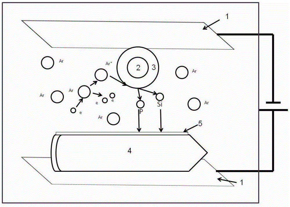
[0018] Put a piece of polysilicon material into the cavity of the magnetron sputtering device after being corroded, cleaned, and dried. Install the prepared phosphorous-doped silicon target, close the door and evacuate to 5×10 -3 Pa, and fill it with argon gas to make the pressure in the cavity reach 1Pa, apply a high voltage of 500KV between the two electrodes, turn on the electric field and magnetic field, start magnetron sputtering, stop sputtering after 30 minutes, and open the sputtering door Rotate the polysilicon material 180° in the circumferential direction, close the sputtering door, repeat the above steps, and continue sputtering, keeping the time at 30 minutes. After the sputtering is completed, take out the polysilicon material and put it into the zone melting silicon single crystal furnace, center the seed crystal and polysilicon, vacuumize, pass argon, preheat, weld, narrow the neck, and put the shoulder until the diameter reaches 80mm. Equal-diameter maintenanc...

Embodiment 2

[0020] Put a piece of polysilicon material into the cavity of the magnetron sputtering device after being corroded, cleaned, and dried. Install the prepared phosphorous-doped silicon target, close the door and evacuate to 5×10 -3 Pa, and fill it with argon gas to make the pressure in the cavity reach 1Pa, apply a high voltage of 500KV between the two electrodes, turn on the electric field and magnetic field, start magnetron sputtering, stop sputtering after 60 minutes, and open the cavity The gate rotates the polysilicon material 180° in the circumferential direction, closes the sputtering gate, repeats the above steps, and continues sputtering, while still controlling the time to 60 minutes. After the sputtering is completed, take out the polysilicon material and put it into the zone melting silicon single crystal furnace, center the seed crystal and polysilicon, vacuumize, pass argon, preheat, weld, narrow the neck, and put the shoulder until the diameter reaches 80mm. Equal...

Embodiment 3

[0022] Grind a piece of polysilicon material, corrode, clean and dry it, then put it into the cavity of the magnetron sputtering apparatus, install the special phosphorus-doped silicon target, close the door and evacuate to 5×10 -3 Pa, and fill it with argon gas to make the pressure in the cavity reach 1Pa, apply a high voltage of 500KV between the two electrodes, turn on the electric field and magnetic field, start magnetron sputtering, stop sputtering after 90 minutes, and open the cavity The gate rotates the polysilicon material 180° along the circumferential direction, closes the sputtering gate, repeats the above steps, and continues sputtering, keeping the time at 90 minutes. After the sputtering is completed, take out the polysilicon material and put it into the zone melting silicon single crystal furnace, center the seed crystal and polysilicon, vacuumize, pass argon, preheat, weld, narrow the neck, and put the shoulder until the diameter reaches 80mm. Equal-diameter m...


PUM


Abstract

The invention relates to a preparation method for a doped float zone silicon crystal. The method comprises that: (1) cone grinding, corrosion, cleaning and drying are performed on a polysilicon material; (2) the polysilicon material is fixed in a cavity of a magnetron sputtering apparatus, a phosphorus-silicon-doped target is arranged, vacuumizing is performed to achieve 5*10<-3> Pa, argon gas is introduced to achieve the pressure in the cavity of 1 Pa, a high voltage of 500 Kv is applied between the two electrodes, argon ions produced through ionization continuously bombard the target, the phosphorus atoms and the silicon atoms in the target obtain energy, sputter, and deposit on the surface of the polysilicon to form a layer of a uniform and compact phosphorus / silicon film, the sputtering is performed for 30-90 min and then is stopped, the sputtering chamber is opened to rotate the polysilicon 180 DEG, the steps are repeated, and the sputtering is continuously performed for the same time; and (3) the polysilicon material is taken out and placed into a float zone silicon crystal furnace, the seed crystal and the polysilicon are centered, steps of vacuumizing, argon gas introduction, preheating, fusion splicing, narrow neck shrinking and crystal diameter achieving are sequentially performed until the equal diameter is maintained, and the ending step is performed. The preparation method has characteristics of low-cost, high production efficiency and no toxicity and harm, wherein the uniformities of the radial resistivity and the axial resistivity are good.

Description

technical field [0001] The invention relates to a method for preparing doped region-fused silicon single crystal, in particular to a method for preparing doped region-fused silicon single crystal by magnetron sputtering. technical background [0002] In the current zone melting silicon single product industry, in order to obtain zone melting silicon single crystal products with low resistivity and controllability, there are mainly two production methods, one is neutron irradiation method, the other is gas phase doping miscellaneous law. Yet these two kinds of methods all have its insurmountable weakness: the cost of neutron irradiation method is high, the finished product cycle is too long, and it is easy to produce irradiation defect; 3 ) has certain toxicity, which brings potential safety hazards, and the resistivity uniformity of the obtained product is not good enough. These disadvantages hinder the respective development of the two methods. Therefore, it is necessary ...

Claims


Application Information

Patent Timeline
Patent Type & Authority Patents(China)
IPC IPC(8): C30B13/00C23C14/35C23C14/06C23C14/16
Inventor 刘志伟闫志瑞陈海滨付斌黄龙辉李明飞
Owner GRINM SEMICONDUCTOR MATERIALS CO LTD
Why Eureka
Try Eureka