Method for generating SRAM layout

A layout and size technology, applied in the field of SRAM layout generation, can solve the problems of low efficiency of the generation method, wrong SRAM layout, time-consuming and energy-consuming, etc., to shorten the implementation time, simplify the design, and reduce the error rate.

Active Publication Date: 2014-08-20
SHANGHAI HUALI MICROELECTRONICS CORP
View PDF6 Cites 2 Cited by
  • Summary
  • Abstract
  • Description
  • Claims
  • Application Information

AI Technical Summary

Problems solved by technology

Although the generation method of the traditional SRAM layout can meet the design requirements of the current SRAM layout, since there are 6 transistors in the SRAM, and each transistor has multiple dimensions that need to be defined, such as gate size, active area size, and injection layer The size of the well layer and the well layer need to be defined. Therefore, the traditional SRAM layout generation method is not efficient, especially when the size of the SRAM needs to be modified, there are many sizes that need to be changed, so human operations often affect the generation of the SRAM layout. Unnecessarily making mistakes and consuming a lot of time and effort

Method used


Image

  • Method for generating SRAM layout
  • Method for generating SRAM layout
  • Method for generating SRAM layout

Examples


Embodiment Construction

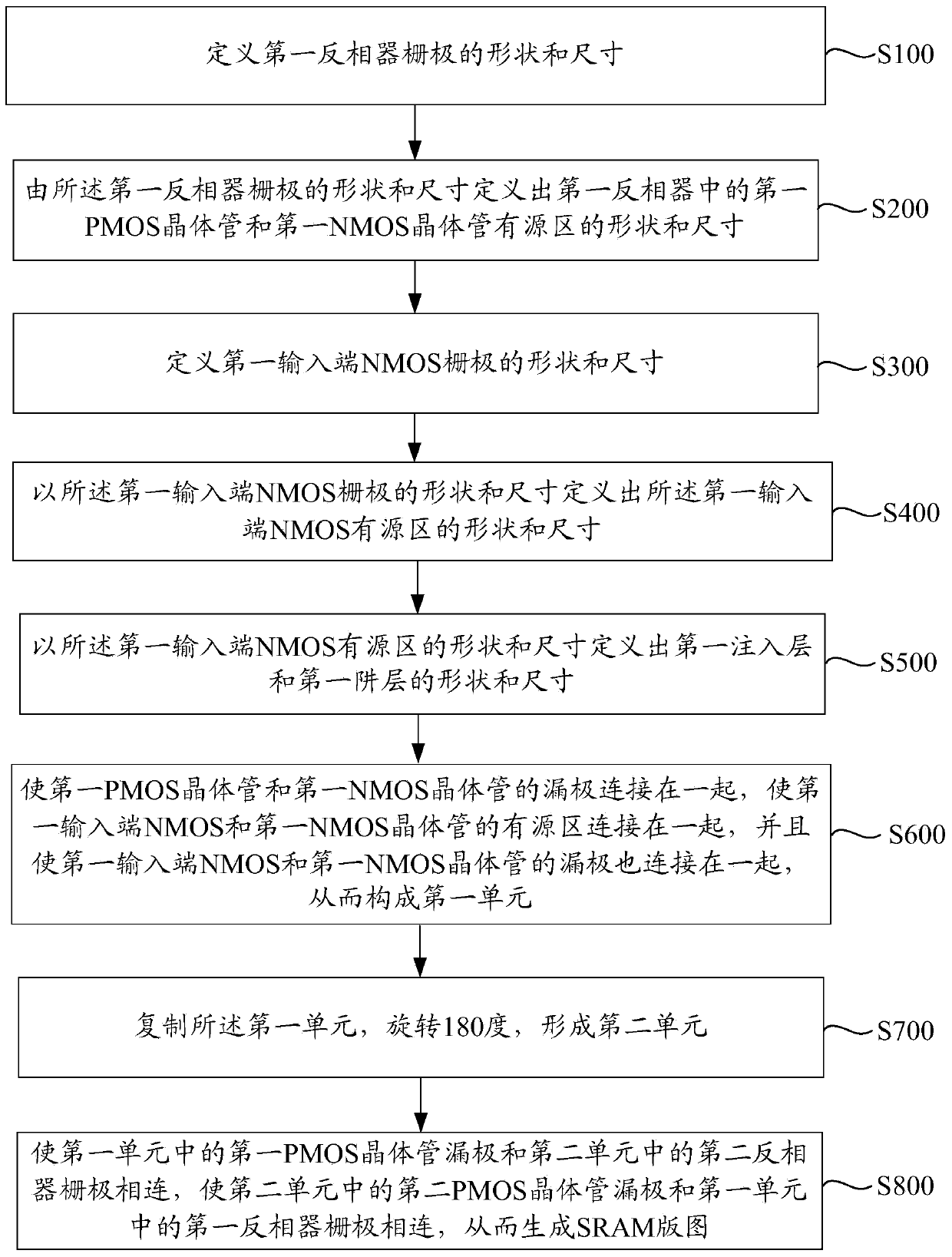
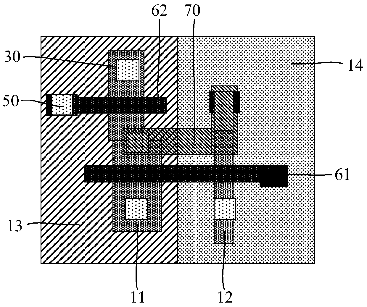
[0024] The method for generating the SRAM layout of the present invention will be described in more detail below in conjunction with the schematic diagram, wherein a preferred embodiment of the present invention is shown, and it should be understood that those skilled in the art can modify the present invention described here, while still realizing the advantages of the present invention Effect. Therefore, the following description should be understood as the broad knowledge of those skilled in the art, but not as a limitation of the present invention.

[0025] In the interest of clarity, not all features of an actual implementation are described. In the following description, well-known functions and constructions are not described in detail since they would obscure the invention with unnecessary detail. It should be appreciated that in the development of any actual embodiment, numerous implementation details must be worked out to achieve the developer's specific goals, such...


PUM


Abstract

The invention provides a method for generating an SRAM layout. The method comprises the steps that firstly, a first unit is formed; secondly, the first unit is copied, so that a second unit is formed; thirdly, the first unit is connected with the second unit, so that an SRAM is formed; finally, identical parameters in the SRAM are grouped, and then the SRAM layout can be automatically generated. In this way, different sizes of SRAM layouts can be effectively generated, design of the SRAM layout is simplified, so that the error rate caused during manual design of the layout is reduced, and the implementation time of the SRAM layout is shortened.

Description

technical field [0001] The invention relates to the field of semiconductor manufacturing, in particular to a method for generating an SRAM layout. Background technique [0002] SRAM (Static Random Access Memory, Static Random Access Memory) is a semiconductor memory that retains data as long as it is powered. SRAM has the advantages of low power consumption, fast data access speed and compatibility with CMOS logic technology, and is widely used in various electronic devices. Therefore, SRAM is an indispensable part of any semiconductor logic process. [0003] A basic SRAM cell consists of two cross-coupled inverters and two access transistors (usually NMOS transistors), which is a typical six-transistor SRAM (6T SRAM). Specifically, the SRAM can be divided into a first inverter (Inverter), a second inverter and two NMOS transistors (abbreviated as NPASS), wherein the first inverter is composed of a first PMOS transistor and a first NMOS transistor, The second inverter is ...

Claims


Application Information

Patent Timeline
Patent Type & Authority Applications(China)
IPC IPC(8): H01L21/8244
CPCH01L27/0207H10B10/12
Inventor 马杰刘梅崔丛丛
Owner SHANGHAI HUALI MICROELECTRONICS CORP
Why Eureka
Try Eureka