Space-time joint modulation Fourier transform imaging spectrometer and manufacturing method
A technology of Fourier transform and imaging spectrometer, applied in the field of manufacturing method and system of infrared imaging spectrometer, can solve problems such as limiting the luminous flux of the system, and achieve the effects of solving the low signal-to-noise ratio of the system, improving luminous flux and improving reliability
- Summary
- Abstract
- Description
- Claims
- Application Information
AI Technical Summary
Problems solved by technology
Method used
Image
Examples
specific Embodiment approach 1
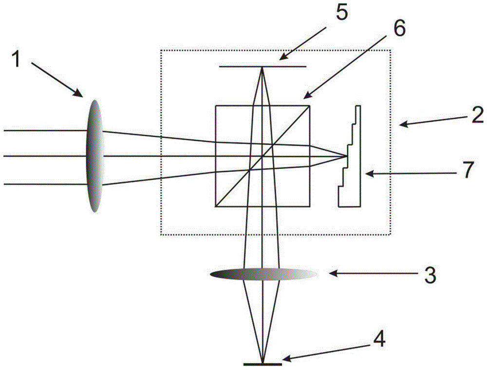
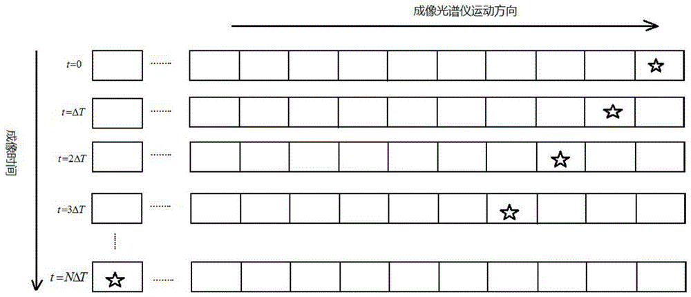
[0029] Specific implementation mode 1. Combination figure 1 and figure 2To illustrate this embodiment, the system structure is composed of a front imaging system 1, an interference system 2, a rear imaging system 3 and a focal plane detector 4. The interference system 2 includes a plane mirror 5, a cube beam splitter 6 and a multi- step micro-mirror 7; in this embodiment, a multi-step micro-mirror 7 is used to replace the moving mirror in the traditional time-modulated Fourier transform imaging spectrometer, so that the whole system is static; After being imaged by the pre-imaging system 1, the emitted light is divided into two beams of coherent light with the same intensity by the cube beam splitter 6. One beam of light is reflected by the cube beam splitter 6 and then imaged on the plane mirror 5, and the other beam passes through After the cube beam splitter 6 is transmitted, it is imaged on the multi-level stepped micro-mirror 7 . Wherein the different reflective surfac...
specific Embodiment approach 2
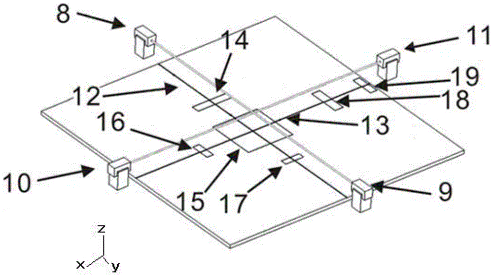
[0039] Specific embodiment two, combine Figure 3 to Figure 5 This embodiment is described. This embodiment is a method for manufacturing the space-time joint modulation Fourier transform imaging spectrometer described in Embodiment 1. The method is implemented by the following steps:
[0040] a. Select the base and make a reference line on the base;
[0041] The specific process is: choose aluminum, copper, titanium, stainless steel or silicon as the base material, make the base material according to the designed size requirements to make the base of the system, and polish the upper surface; the roughness of the polished surface is less than 10 microns, and the plane The degree is less than or equal to 50 microns. Such as image 3 As shown, according to the analysis and calculation, the reference lines perpendicular to each other are made on the polished substrate by the precision machining method or the photolithography and etching method based on MOEMS technology as the r...
PUM
 Abstract
Description
Claims
Application Information


