Method and system for detecting semiconductor device, semiconductor device and manufacturing method thereof

A technology for semiconductors and conductors, applied in the design of new inspection patterns, in the field of identifying defects in deposited metal layers, and can solve the problems of time-consuming defect detection technology, redundancy, etc.

Inactive Publication Date: 2014-08-27
MACRONIX INT CO LTD
View PDF3 Cites 0 Cited by
  • Summary
  • Abstract
  • Description
  • Claims
  • Application Information

AI Technical Summary

Problems solved by technology

Other methods to detect internal defects often require lengthy and time-consuming defect detection techniques

Method used


Image

  • Method and system for detecting semiconductor device, semiconductor device and manufacturing method thereof
  • Method and system for detecting semiconductor device, semiconductor device and manufacturing method thereof
  • Method and system for detecting semiconductor device, semiconductor device and manufacturing method thereof

Examples


Embodiment Construction

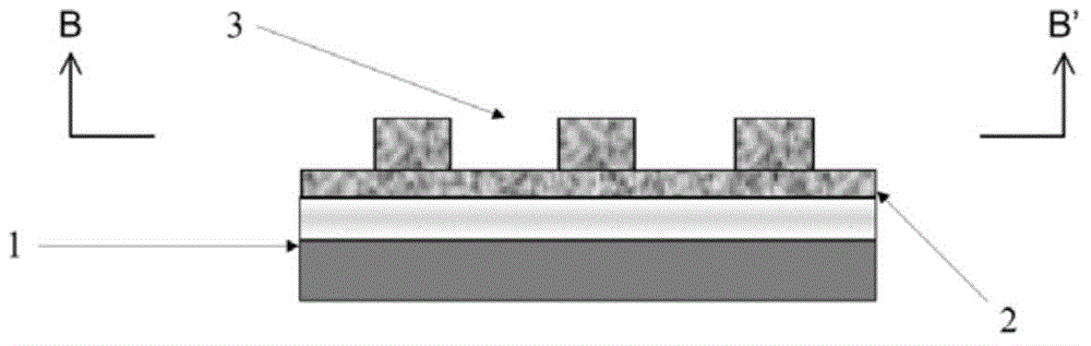
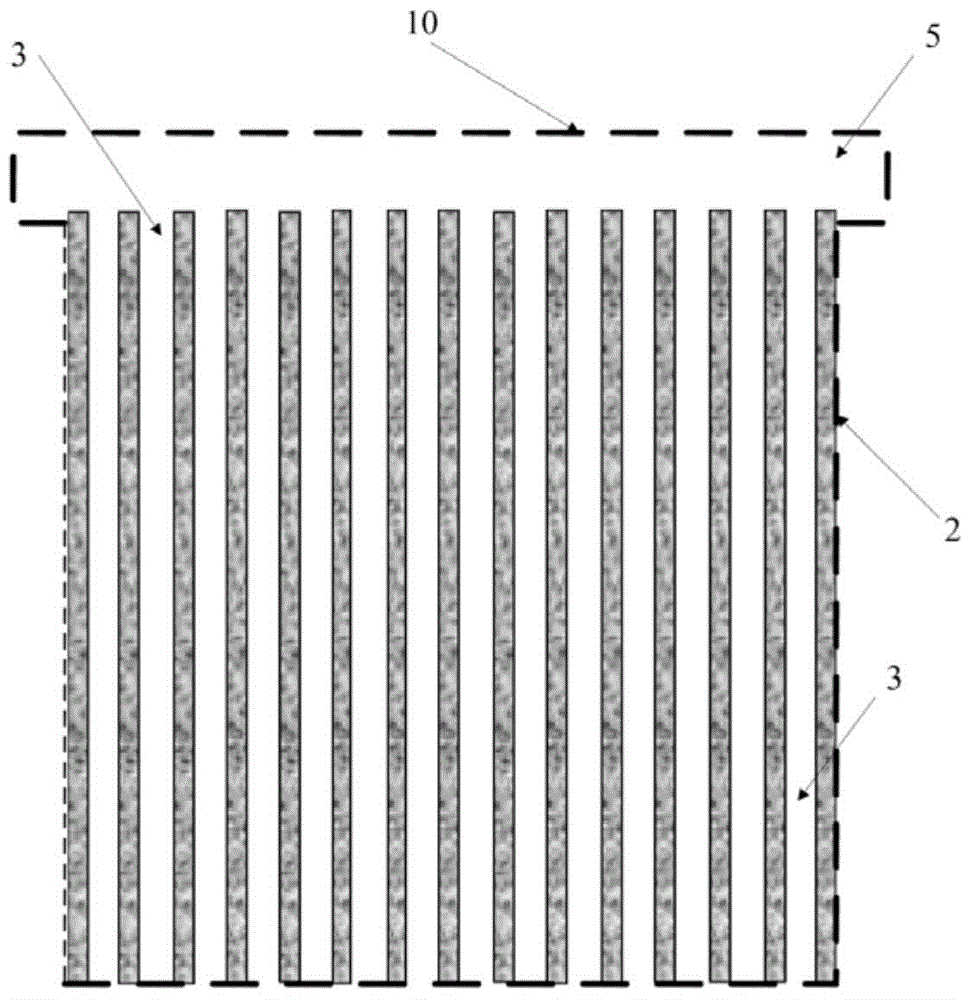
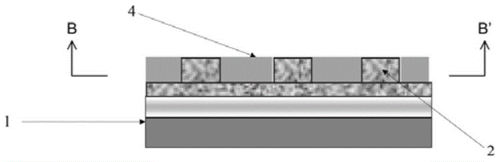
[0068] In order to further explain the technical means and effects of the present invention to achieve the intended purpose of the invention, the method and system for detecting semiconductor devices and the detection of semiconductor devices and semiconductor devices according to the present invention will be described below in conjunction with the accompanying drawings and preferred embodiments. The specific implementation, method, steps, structure, features and effects of the pattern design and its manufacturing and utilization method are described in detail below.

[0069] As used in the specification and in the claims, singular forms include plural words unless the context clearly dictates otherwise. For example, reference to "a semiconductor device" includes a plurality of such semiconductor devices.

[0070] Although specific terms are employed herein, they are used in a common and descriptive sense and not for purposes of limitation only. All terms used herein, includ...


PUM


Abstract

The invention relates to a method and a system for detecting a semiconductor device, the semiconductor device and a manufacturing method thereof. The invention provides a method and a system for detecting faults in a semiconductor, a semiconductor device or a substrate. The invention also provide a semiconductor, a semiconductor device or a substrate having novel test patterns and / or designs. The semiconductor, the semiconductor device or the substrate having a plurality of line patterns generates a reaction. The line patterns are corresponding to a reaction stimulant (such as electronic beam radiation). The reaction stimulant can comprise an electronic beam radiation. The reaction generates an image file which can be collected and processed to generate an image indicating surface and / or internal faults.

Description

technical field [0001] The present invention relates to a semiconductor device. In particular, it relates to a novel inspection pattern and a method of using the inspection pattern to identify defects in deposited metal layers. Background technique [0002] The fabrication of semiconductor devices usually requires creating patterns of conductive metal to interconnect different layers of the semiconductor device. This may involve a "mosaic process". Therefore, circuit patterns may be formed on or in a dielectric layer on a surface of the semiconductor device. For example, a circuit pattern can be formed by etching an insulating layer and filling it with a conductive metal. A selective removal process such as mechanical polishing or chemical mechanical polishing can be used to ensure that the conductive metal is disposed in the etched circuit pattern. [0003] A continuing trend in the semiconductor industry is towards higher device densities without compromising device pe...

Claims


Application Information

Patent Timeline
Patent Type & Authority Applications(China)
IPC IPC(8): H01L21/66H01L23/544H01L21/768G01N23/22
CPCH01L22/12G01N23/22G01N2223/646H01L22/30H01L22/34
Inventor 庄严洪哲伦李筱玲
Owner MACRONIX INT CO LTD
Why Eureka
Try Eureka