AlGaN/GaN heterojunction field effect transistor

A heterojunction field effect and transistor technology, which is applied to semiconductor devices, electrical components, circuits, etc., can solve the problems of device threshold voltage and output current reduction, leakage current exceeding the predetermined range, and device reliability reduction, etc. The effect of reducing channel resistance, avoiding current collapse effect, improving breakdown voltage and device reliability

Active Publication Date: 2014-08-27
XIDIAN UNIV
View PDF4 Cites 17 Cited by
  • Summary
  • Abstract
  • Description
  • Claims
  • Application Information

AI Technical Summary

Problems solved by technology

[0005] In order to solve the breakdown of the device caused by the peak electric field at the gate edge of the AlGaN / GaN high electron mobility transistor in the prior art, the leakage current exceeds the predetermined range, the current collapse effect occurs, and the threshold voltage and output current of the device decrease. A series of problems such as reduced device reliability, the present invention provides a novel AlGaN / GaN heterojunction field effect transistor

Method used


Image

  • AlGaN/GaN heterojunction field effect transistor

Examples


Embodiment Construction

[0029] In order to make the technical problems, technical solutions and advantages to be solved by the present invention clearer, a detailed description will be given below in conjunction with the accompanying drawings and specific embodiments.

[0030] The invention provides a novel AlGaN / GaN high electron mobility transistor with passivation layer charge compensation for the problem of peak electric field at the gate edge of the existing AlGaN / GaN high electron mobility transistor.

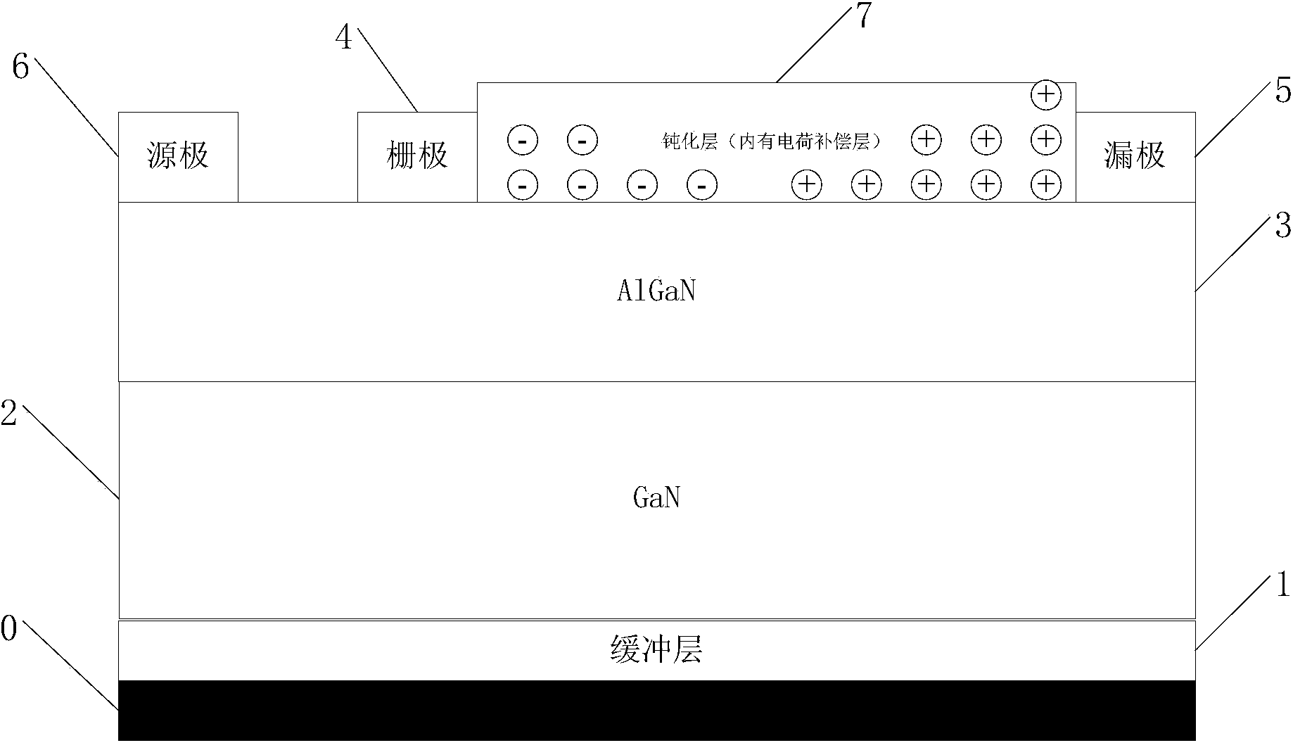
[0031] Its structure is as figure 1 As shown, it mainly includes: a semi-insulating substrate 0; a buffer layer 1 epitaxially grown on the semi-insulating substrate; a GaN buffer layer 2 epitaxially grown on the surface of the buffer layer 1; a heteroepitaxially grown AlGaN layer 3 on the GaN buffer ; the gate 4, the drain 5 and the source 6 located on the AlGaN layer; the passivation layer 7 located between the gate and the drain, wherein the passivation layer contains a charge compensation lay...


PUM


Abstract

The invention discloses a novel AlGaN / GaN high-electronic-mobility transistor with the passivation layer charge compensation function. According to the novel crystal structure, charges are injected into a surface passivation layer between the grid electrode and the drainage electrode of the transistor, so that a charge compensation layer is formed, the charges exist on the surface of the transistor, surface electric fields are re-distributed through the electric field modulation effect on the premise that the AlGaN / GaN heterojunction polarization effect is not affected, a new electric field peak is generated, in this way, high electric fields on the edge of the grid electrode and at the drainage end are lowered, the surface electric fields tend to be even, and compared with a traditional structure, the breakdown voltage and the reliability of devices are improved remarkably; in addition, due to the fact that the charge compensation layer has the charge compensation function, the carrier concentrations of channels are re-distributed, the on resistance of the devices is reduced, and the output current is increased.

Description

technical field [0001] The invention relates to the technical field of semiconductor devices, in particular to an AlGaN / GaN heterojunction field effect transistor. Background technique [0002] Due to the limitations of the first two generations of semiconductor materials represented by Si and GaAs, the third generation of wide-bandgap semiconductor materials has developed rapidly because of their excellent performance. As one of the cores of the third-generation semiconductor materials, GaN material is special in that it has a polarization effect compared with Si, GaAs and silicon carbide (SiC). AlGaN / GaN high electron mobility transistors have been developed by taking advantage of this special performance. AlGaN / GaN HEMTs are GaN-based microelectronic devices based on AlGaN / GaN heterojunction materials. AlGaN / GaN heterojunction forms a high-density two-dimensional electron gas (2DEG) at the heterojunction interface through spontaneous polarization and piezoelectric polari...

Claims


Application Information

Patent Timeline
Patent Type & Authority Applications(China)
IPC IPC(8): H01L29/778H01L29/06
CPCH01L29/0619H01L29/0638H01L29/7787
Inventor 段宝兴袁嵩杨银堂郭海君
Owner XIDIAN UNIV
Why Eureka
Try Eureka