
A preparation method of a low dielectric constant composite film containing nanopores

A low dielectric constant, composite thin film technology, applied in the direction of circuits, electrical components, electrical solid devices, etc., can solve the problems of mechanical property degradation, limit the application of low-k thin films, and deteriorate the thermal stability of thin films, etc., to achieve excellent mechanical properties performance, good insulation performance, and the effect of low dielectric constant

Inactive Publication Date: 2017-01-11
FUDAN UNIV
View PDF7 Cites 0 Cited by
  • Summary
  • Abstract
  • Description
  • Claims
  • Application Information

AI Technical Summary

Problems solved by technology

However, the introduction of too many organic groups and micropores will lead to poor thermal stability and degradation of mechanical properties of the film, which limits the application of low-k films in back-end interconnection processes

Method used


Image

  • A preparation method of a low dielectric constant composite film containing nanopores
  • A preparation method of a low dielectric constant composite film containing nanopores

Examples


Embodiment 1

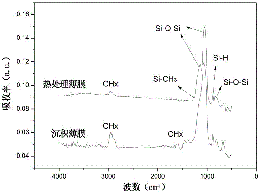
[0018] The substrate temperature was set at 200 °C, the working pressure in the reaction chamber was 3 Torr, the deposition power was 300 W; the mass ratio of TEOS and LIMO was 1:1, and the vaporization temperatures were 160 °C and 100 °C, respectively; helium was used as the carrier gas , the flow rates were 2000 sccm and 5000 sccm, and the inorganic-organic composite thin film was deposited. The deposited film is thermally annealed at different temperatures in an argon (Ar) atmosphere, the pressure is less than 0.3 Torr, and the annealing time is 1 hour.

[0019] Thin film performance measurement: The film thickness and refractive index are measured by ellipsometer, the measurement wavelength range is 250 nm~800 nm, and the Cauthy model is used for fitting. In order to measure the electrical properties of the above-mentioned thin film, the present invention uses a low-resistivity silicon wafer (resistivity 0.001~0.005 Ω·cm) as the substrate, and uses electron beam evaporated...

Embodiment 2

[0024] The substrate temperature was set at 200 °C, the working pressure in the reaction chamber was 3 Torr, and the deposition power was 300 W; different mass ratios of TOES and LIMO were used to obtain a clean low-resistivity silicon wafer (resistivity 0.001-0.005 Ω• cm) as the substrate, a series of inorganic-organic composite films were deposited, and in nitrogen (N 2 ) atmosphere for thermal annealing, the pressure is about one atmosphere, the annealing temperature is 450 °C, and the annealing time is 1.5 hours. As shown in Table 2, the refractive index of the obtained films ranged from 1.364 to 1.369, the Young's modulus ranged from 6.65 GPa to 8.79 GPa, and the hardness ranged from 0.59 GPa to 0.92 GPa. The electrical properties of the obtained film were tested at 100°C, the k value was 2.60~2.75, and the leakage current density at 1 MV / cm was all at 10 -9 A / cm 2 Magnitude.

[0025] Table 2

[0026] .

Embodiment 3

[0028] Set the substrate temperature at 200 °C, the working pressure in the reaction chamber at 3 Torr, the mass ratio of TEOS and LIMO at 1:1, and use a clean low-resistivity silicon wafer (0.001-0.005 Ω cm) as the substrate , change the deposition power (respectively 350 W, 450 W, 550 W), and deposit a series of thin films. Then, the obtained thin film was placed in an Ar atmosphere for thermal annealing treatment, the gas pressure was less than 0.3 Torr, the annealing temperature was 425° C., and the annealing time was 4 hours. The electrical properties of the heat-treated film are shown in Table 3, and the test temperature is room temperature. As the PECVD RF power increased from 350 W to 550 W, the dielectric constant of the obtained film increased from 2.71 to 2.90, and the leakage current density at 1 MV / cm field strength was located at 8.06×10 -9 A / cm 2 ~1.23×10 -8 A / cm 2 within range.

[0029] table 3

[0030] .


PUM

PropertyMeasurementUnit
breakdown field strengthaaaaaaaaaa
electrical resistivityaaaaaaaaaa
diameteraaaaaaaaaa

Abstract

The invention belongs to the technical field of integrated circuit manufacture, and particularly relates to a method for preparing a low-dielectric-constant composite film with nanometer holes. tetraethoxysilane and dipentene serve as precursors, the technology that chemical vapor deposition is enhanced through plasma is adopted, technological parameters such as substrate temperature, radio-frequency power, working pressure intensity in a reaction chamber and the precursor ratio are controlled in the deposition process, an inorganic-organic composite film is obtained through deposition; proper thermal annealing is conducted on the inorganic-organic composite film, so that parts of organic components are thermally decomposed, and the low-dielectric-constant composite film with the nanometer holes is obtained. The dielectric constant of the film ranges from 2.5 to 2.9, under 1 MV / cm field strength, the leakage current density ranges from 10<-8> A / cm<2> to 10<-9> A / cm <2> at the order of magnitude, breakdown field strength is larger than 2 MV / cm, and the mechanical property is excellent. The method is easy to operate and completely compatible with an existing integrated circuit rear-end interconnection technology and is an ideal candidate of an interconnection medium.

Description

technical field [0001] The invention belongs to the technical field of integrated circuit manufacturing, and in particular relates to a preparation method of a low dielectric constant composite film containing nanopores, which is applied to interlayer dielectrics in copper interconnection. Background technique [0002] With the development of integrated circuit technology, chips with high speed, high device density, low power consumption and low cost have increasingly become the main products of VLSI. At this time, the density of wires in the chip continues to increase, and the width and spacing of wires continue to decrease, which leads to the parasitic effects of resistance (R) and capacitance (C) in the chip's back-end interconnection becoming more and more obvious. At present, the industry has generally used copper (Cu) instead of aluminum (Al) for wiring to reduce resistance; and the use of low dielectric constant (low-k) materials to replace traditional silicon dioxide...

Claims


Application Information

Patent Timeline
Patent Type & Authority Patents(China)
IPC IPC(8): H01L21/768C23C16/44C23C16/513
CPCC23C16/44C23C16/513H01L21/7682H01L2221/1047
Inventor 丁士进谭再上范仲勇张卫
Owner FUDAN UNIV
Learn More