AlGaN film grown on Si substrate, preparation method and application thereof
A technology for substrates and thin films is applied in the field of metal organic chemical vapor deposition combined with pulsed laser deposition to synthesize films. and thermal mismatch amplification, the effect of reducing manufacturing cost and shortening nucleation time
- Summary
- Abstract
- Description
- Claims
- Application Information
AI Technical Summary
Problems solved by technology
Method used
Image


Examples
Embodiment 1
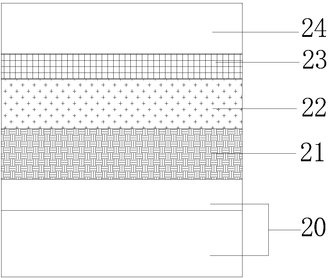
[0029] Reference figure 1 The AlGaN film grown on the Si substrate of the present invention includes the Si substrate 11 and the AlGaN film 12.
[0030] The AlGaN film grown on the Si substrate is prepared by the following method:
[0031] (1) Selection of substrate and crystal orientation: using a Si substrate, select a crystal orientation of 0.5° from the (111) plane to the (100) direction;
[0032] (2) Using metal organic chemical vapor deposition process to grow Al atomic layer, the process conditions are: substrate temperature is 960℃, reaction chamber pressure is 50torr, TMAl is introduced, flow rate is 250sccm, two to three layers of Al atomic layer are laid to isolate Si substrate and NH 3 Contact to prevent the formation of SiN x ;
[0033] (3) Nitriding the Al atomic layer, the process conditions are: the substrate temperature is 860°C, the reaction chamber pressure is 100torr, and NH is introduced 3 , The flow rate is 5slm, the nitriding time is 6min;
[0034] (4) Using puls...
Embodiment 2
[0036] On the basis of Example 1, the AlGaN thin film grown on the Si substrate was prepared by the following method:
[0037] (1) Selection of substrate and crystal orientation: using a Si substrate, select a crystal orientation of 0.5° from the (111) plane to the (100) direction;
[0038] (2) A metal-organic chemical vapor deposition process is used to grow the Al atomic layer. The process conditions are: the substrate temperature is 860°C, the reaction chamber pressure is 100 torr, TMAl is introduced, the flow rate is 200 sccm, and two to three Al atomic layers are laid to isolate Si substrate and NH 3 Contact to prevent the formation of SiN x ;
[0039] (3) Nitriding treatment is performed on the Al atomic layer, the process conditions are: the substrate temperature is 960℃, the reaction chamber pressure is 50torr, and NH is introduced. 3 , The flow rate is 15slm, the nitriding time is 3min;
[0040] (4) Using pulsed laser deposition process to grow AlGaN thin film, the process co...
Embodiment 3
[0042] This embodiment is modified on the basis of embodiment 1. The difference is: after the substrate and crystal orientation are selected, and before the Al atomic layer is grown, the substrate is subjected to surface cleaning and annealing treatment steps in sequence. The specific method as follows:
[0043] Surface cleaning treatment: the Si substrate is first ultrasonically cleaned in acetone solution, then ultrasonically cleaned in deionized water; then ultrasonically cleaned in isoacetone solution; then ultrasonically cleaned in hydrofluoric acid solution, and then deionized Soak in water; then soak the Si substrate in a mixed solution of sulfuric acid and hydrogen peroxide; finally soak the Si substrate in hydrofluoric acid, rinse with deionized water, and blow dry with nitrogen.
[0044] Annealing treatment: Place the substrate in an ultra-high vacuum growth chamber and bake it at 1000-1100°C for 5-15 minutes.
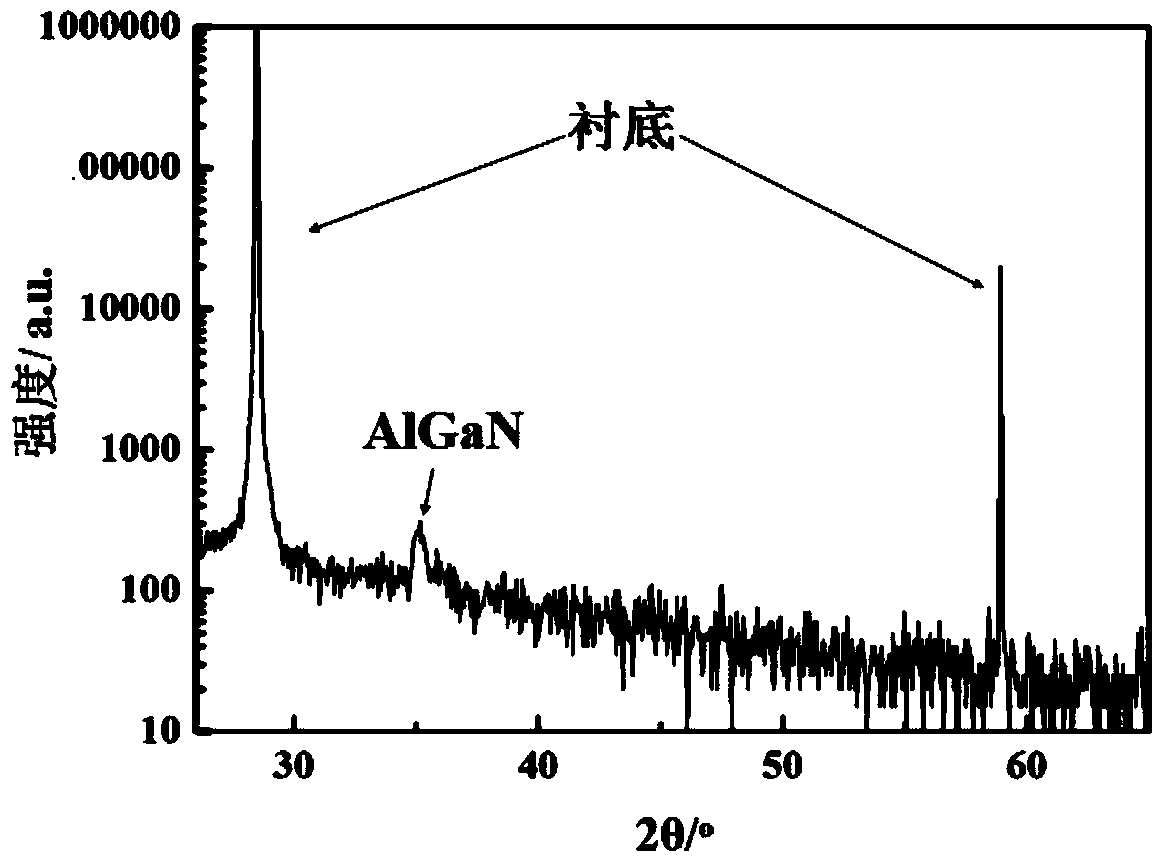
[0045] Reference figure 2 It can be seen from the X-ray surf...
PUM
 Abstract
Description
Claims
Application Information
 - R&D Engineer
- R&D Manager
- IP Professional
- Industry Leading Data Capabilities
- Powerful AI technology
- Patent DNA Extraction
Browse by: Latest US Patents, China's latest patents, Technical Efficacy Thesaurus, Application Domain, Technology Topic.
© 2024 PatSnap. All rights reserved.Legal|Privacy policy|Modern Slavery Act Transparency Statement|Sitemap