Duty ratio conversion circuit and conversion method

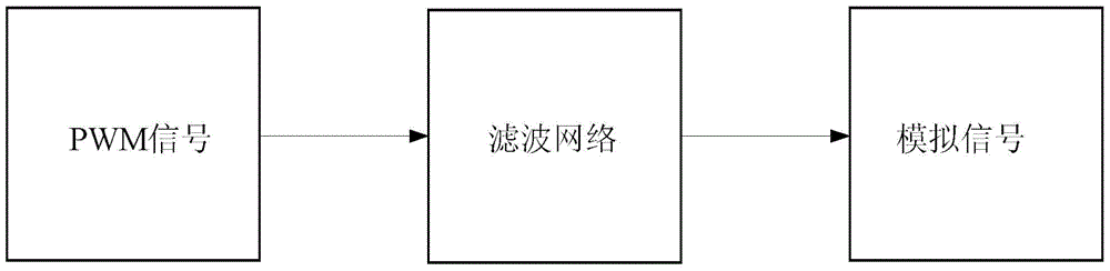
A conversion circuit and duty cycle technology, applied in the direction of output power conversion devices, electrical components, etc., can solve the problems of large output ripple, reduced service life of conversion circuit, response speed and output ripple cannot be solved at the same time, to achieve Fast response and improved service life

Active Publication Date: 2016-09-14
SILERGY SEMICON TECH (HANGZHOU) CO LTD
View PDF6 Cites 0 Cited by
  • Summary
  • Abstract
  • Description
  • Claims
  • Application Information

AI Technical Summary

Problems solved by technology

[0004] However, there is a problem in the duty-to-analog signal conversion circuit implemented by the filtering network similar to the prior art, that is, the conversion response speed and the output ripple cannot be solved at the same time
The reason is that only when the time constant of the resistor R and the capacitor C is much greater than the frequency of the PWM signal, can the output analog signal be approximated as a DC signal, which solves the problem of large output ripple. However, due to the resistance R and the capacitor C The time constant of the conversion circuit is very large, which will cause the problem of slow response speed of the conversion circuit. The two cannot be balanced, and the large-capacity capacitor will increase the volume and manufacturing cost of the conversion circuit, and will also reduce the service life of the conversion circuit.

Method used


Image

  • Duty ratio conversion circuit and conversion method
  • Duty ratio conversion circuit and conversion method
  • Duty ratio conversion circuit and conversion method

Examples


Embodiment 1

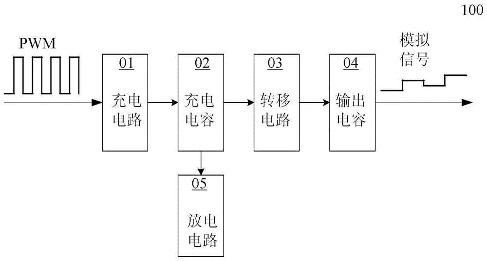
[0041] Please refer to figure 2 , in this embodiment, a duty cycle conversion circuit 100 is proposed for converting a PWM signal into an analog signal. Specifically, the duty ratio conversion circuit 100 includes a charging circuit 01 , a charging capacitor 02 , a transfer circuit 03 , an output capacitor 04 and a discharging circuit 05 .

[0042] In each cycle of the PWM signal, when the PWM signal is at a high level, the charging circuit 01 outputs a charging current to charge the charging capacitor 02;

[0043] When the PWM signal is at low level, the charging current stops charging the charging capacitor 02, and within the transfer time period, the voltage on the charging capacitor 02 is output to the output capacitor through the transfer circuit 03 04 ; during the discharge time period, the charging capacitor 02 is discharged through the discharging circuit 05 to reduce the voltage on the charging capacitor 02 to an initial voltage. The initial voltage here refers to ...

Embodiment 2

[0048] Please refer to image 3 , in this embodiment, an optimized duty ratio conversion circuit 200 of Embodiment 1 is proposed. Specifically, the charging circuit 01 includes a controlled current source A, and the specific controlled current source A is a voltage-controlled current source controlled by a PWM signal. When the PWM signal is at a high level, a voltage V PWM Controlling the controlled current source A to output a charging current I to the charging capacitor 02 1 , when the PWM signal is low, there is no voltage V PWM Control the controlled current source A, then the controlled current source A has no charging current I 1 output.

[0049] In order to ensure the stability and accuracy of the charging process, the charging circuit of this embodiment further includes a charging control switch connected in series with the controlled current source A. Specifically, the charging control switch described in this embodiment includes a charging control switch S1, and ...

Embodiment 3

[0059] In this embodiment, another optimized duty cycle conversion circuit 300 of Embodiment 1 is proposed. For details, please refer to Figure 4 The only difference between this embodiment and the second embodiment is the composition of the charging circuit 01 , and the other parts are the same as those of the second embodiment, and will not be repeated here. In this embodiment, the charging circuit 01 includes a current source and a charging control switch. The specific current source can be a constant current source or any other current source. In this embodiment, the current source is Constant current source A, used to output constant charging current I 1 The charging control switch includes a charging control switch S1, one end of the charging control switch S1 is connected to the constant current source A, and the other end is connected to the charging capacitor O2, and the on and off of the charging control switch S1 is controlled by the PWM signal. When the PWM signa...


PUM


Abstract

The invention provides a duty cycle conversion circuit and method. The method comprises the following steps: charging a charging capacitor with a charging current when a PWM (Pulse-Width Modulation) signal is at high level; stopping charging when the PWM signal is at low level; transferring the voltage from the charging capacitor to an output capacitor and then converting to obtain a simulating signal; recovering the electric quantity in the charging capacitor into initial voltage; cycling in sequence until the PWM signal in each cycle is converted into the simulation signal before the cycle is ended. The duty cycle conversion method has the characteristics that the respond speed is fast, the converted simulating signal is able to remain zero order, and the problem of large ripple wave caused by insufficient filter depth of the converting circuit in the prior art is avoided; in addition, the large-capacity energy storing element in the traditional converting circuit is removed, thus the chip integration can be performed conveniently, the size of an electronic device and the manufacturing cost can be reduced, and the service life is also prolonged as the same time.

Description

technical field [0001] The invention relates to a switching power supply, in particular to a duty cycle conversion circuit and a conversion method. Background technique [0002] In a switching power supply, the first part of the control circuit compares the output voltage or output current with a sawtooth signal to generate a PWM (Pulse-Width Modulation) signal or PFM (Pulse Frequency Modulation) signal with a duty cycle. Change, Pulse Frequency Modulation) signal. The second part of the control circuit receives a PWM signal or a PFM signal as an input signal, and then generates a control signal for switching the switches in the power stage circuit on or off. The second part of the control circuit and the power stage circuit together can be considered as a duty cycle conversion circuit. The duty cycle conversion circuit converts the PWM signal or the PFM signal into an analog signal, that is, the DC output voltage or the DC output power of the switching power supply. Duty...

Claims


Application Information

Patent Timeline
Patent Type & Authority Patents(China)
IPC IPC(8): H02M1/00
Inventor 曹何金生赵晨
Owner SILERGY SEMICON TECH (HANGZHOU) CO LTD
Why Eureka
Try Eureka