
Method for manufacturing shielding of organic light-emitting device

A technology of an organic light-emitting device and a manufacturing method, applied in the field of shielding manufacturing, can solve the problems of uneven shielding, incomplete etching, deformation of openings, etc.

Inactive Publication Date: 2014-09-17
华映视讯(吴江)有限公司 +1
View PDF6 Cites 1 Cited by
  • Summary
  • Abstract
  • Description
  • Claims
  • Application Information

AI Technical Summary

Problems solved by technology

However, since chemical etching is isotropic etching, thinner substrates must be used to form openings with smaller top-view dimensions
If a thicker substrate is used, incomplete etching may occur, resulting in smaller openings in the top view not completely penetrating the substrate
[0003] However, when the screen is stretched using a thinner base material, the middle part of the screen may collapse, causing the screen to be uneven and the opening to be deformed

Method used


Image

  • Method for manufacturing shielding of organic light-emitting device
  • Method for manufacturing shielding of organic light-emitting device
  • Method for manufacturing shielding of organic light-emitting device

Examples


Embodiment Construction

[0034] The present invention provides a method for manufacturing a shield for an organic light emitting device. In one embodiment, the organic light emitting device is an organic light emitting diode device, which includes one or more organic light emitting diodes. In one embodiment, the mask is used to form the organic light-emitting layer in an organic light-emitting diode. For example, the aforementioned organic light-emitting layer can be formed by using an evaporation process in conjunction with the mask manufactured according to the embodiment of the present invention. The material of the organic light-emitting layer can be, for example, red, green or blue organic light-emitting materials.

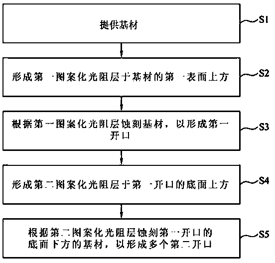
[0035] figure 1 is a flowchart of a method of manufacturing a shield according to the present invention. Such as figure 1 As shown, the manufacturing method of the mask includes providing a substrate (step S1), forming a first patterned photoresist layer (step S2), etching the su...


PUM

PropertyMeasurementUnit
Thicknessaaaaaaaaaa

Abstract

A method for manufacturing shielding of an organic light-emitting device includes the steps of forming a first patterning photoresistance layer above a first surface of a base material, etching the base material according to the first patterning photoresistance layer to form a first opening, wherein the first opening is provided with a bottom face, forming a second patterning photoresistance layer above the bottom face of the first opening, and etching the base material below the bottom face of the first opening according to the second patterning photoresistance layer to form a plurality of second openings which are separated from one another and penetrate through the base material to be directly communicated with the first opening.

Description

technical field [0001] The present invention relates to a method for manufacturing a shield, and in particular to a method for manufacturing a shield for an organic light-emitting device. Background technique [0002] Currently, masks used in the manufacture of organic light-emitting devices usually use chemical etching to produce desired patterns on the substrate. In order to increase the pixel density of the organic light-emitting device (eg, pixel per inch (PPI, pixel per inch)), the smaller the opening size of the shielding, the better. However, since the chemical etching is isotropic etching, a thinner substrate must be used to form an opening with a smaller top view size. If a thicker substrate is used, incomplete etching may occur, causing the opening with a smaller size in the top view to fail to completely penetrate the substrate. [0003] However, when the shield prepared by using a thinner substrate is stretched, the middle part of the shield may collapse downwa...

Claims


Application Information

Patent Timeline
IPC IPC(8): H01L51/56
CPCH10K71/00
Inventor 黄金海赖冠宇黄思齐冯捷威
Owner 华映视讯(吴江)有限公司
Learn More