Supercharge Your Innovation With Domain-Expert AI Agents!

Semiconductor Device And Method Of Manufacturing Same

A semiconductor and lattice position technology, which is applied in semiconductor/solid-state device manufacturing, semiconductor devices, electrical components, etc., can solve problems such as deep energy levels, difficult to reduce resistance, and low solid solution limit

Inactive Publication Date: 2014-09-24
KK TOSHIBA
View PDF1 Cites 0 Cited by
  • Summary
  • Abstract
  • Description
  • Claims
  • Application Information

AI Technical Summary

Problems solved by technology

[0005] On the other hand, due to the low solid solution limit of impurities and the deep energy level in the band gap formed by impurities, SiC makes it difficult to reduce the resistance of p-type impurity regions or n-type impurity regions.

Method used


Image

  • Semiconductor Device And Method Of Manufacturing Same
  • Semiconductor Device And Method Of Manufacturing Same
  • Semiconductor Device And Method Of Manufacturing Same

Examples


no. 1 approach )

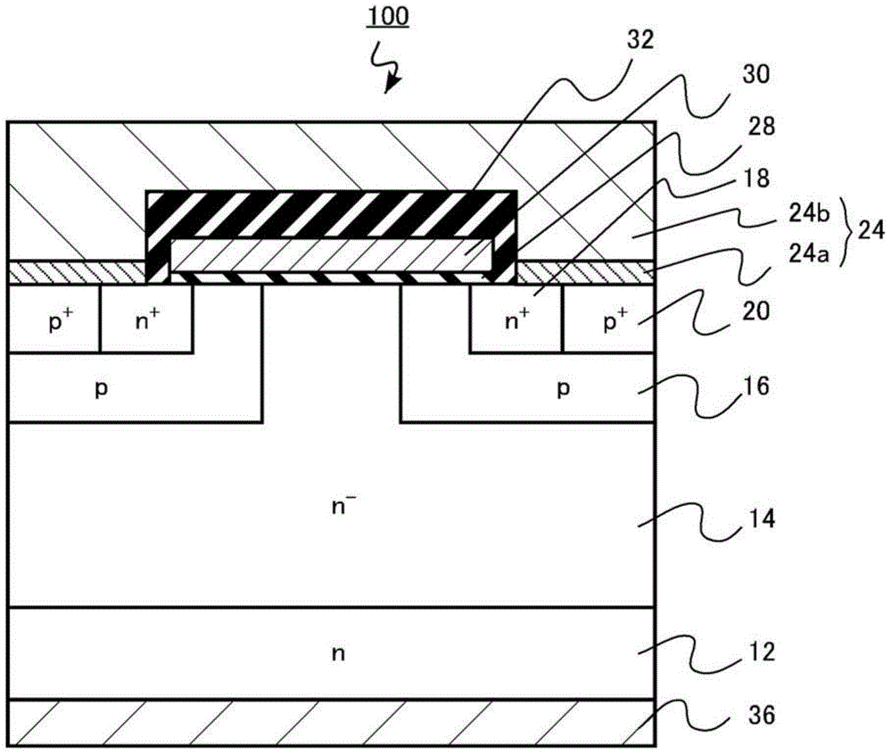
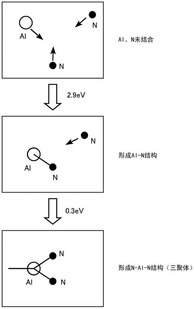
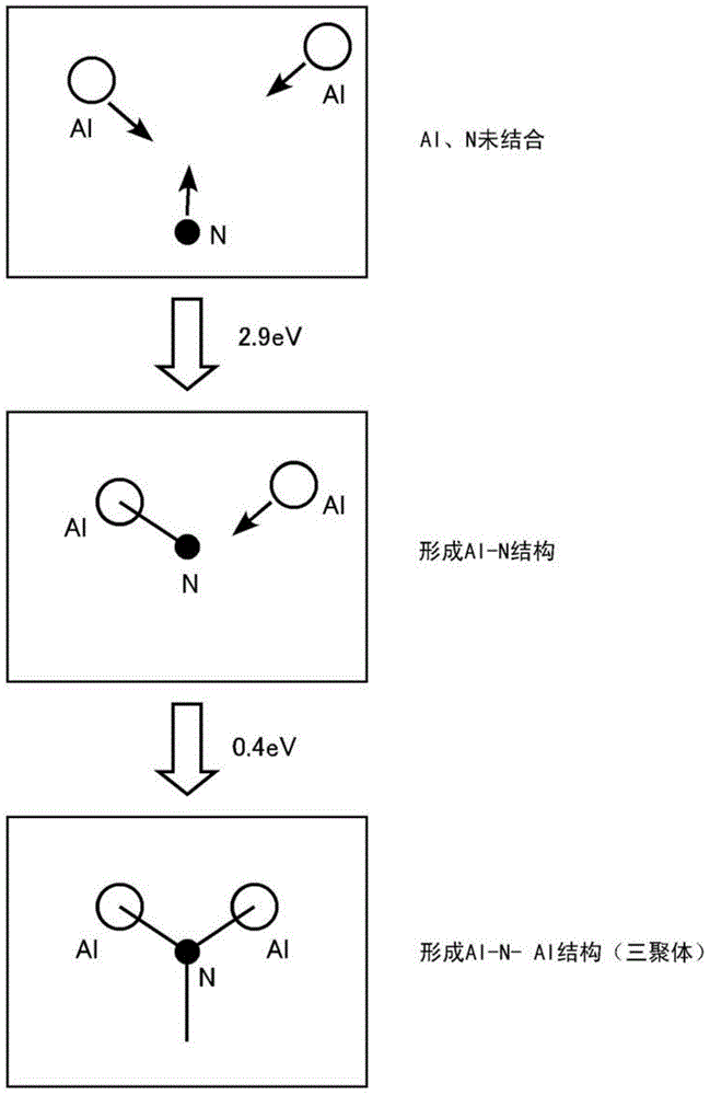
[0037] The semiconductor device of this embodiment includes an n-type SiC substrate having a first surface and a second surface, an n-type SiC layer provided on the first surface side of the SiC substrate, and a p-type first SiC layer formed on the surface of the SiC layer. A SiC region and an n-type second SiC region formed on the surface of the first SiC region. In addition, a p-type third SiC region is provided. The p-type third SiC region is formed on the surface of the first SiC region and contains p-type impurities and n-type impurities. When recorded as element D, the combination of element A and element D is at least one of the combination of Al (aluminum), Ga (gallium), or In (indium) and N (nitrogen), and the combination of B (boron) and P (phosphorus). A combination in which the ratio of the concentration of element D to the concentration of element A (concentration D / concentration A) that constitutes the above combination is greater than 0.33 and less than 0.995, a...

no. 2 approach )

[0160] except in n + The semiconductor device of this embodiment is the same as that of the first embodiment except that the p-type impurity and n-type impurity are also co-doped in the second SiC region. Therefore, the description of the contents overlapping with the first embodiment will be omitted.

[0161] In the semiconductor device of this embodiment mode, in figure 1 MOSFET100, the n + Type second SiC region (source region) 18 is co-doped with p-type impurities and n-type impurities. Also, when the p-type impurity in the second SiC region (source region) 18 is denoted as element A and the n-type impurity is denoted as element D, the combination of element A and element D is Al (aluminum), Ga (gallium) Or at least one combination of a combination of In (indium) and N (nitrogen) and a combination of B (boron) and P (phosphorus). For example, element A is Al and element D is N.

[0162] In the MOSFET of this embodiment, at n + The second SiC region (source region) 18...

no. 3 approach )

[0182] The semiconductor device of this embodiment includes an n-type SiC substrate having a first surface and a second surface, and an n-type SiC layer provided on the first surface side of the SiC substrate. In addition, a p-type SiC region is provided. The p-type SiC region is formed on the surface of the SiC layer and contains p-type impurities and n-type impurities. When the p-type impurity is expressed as element A and the n-type impurity is expressed as element D, The combination of element A and element D is at least one of the combination of Al (aluminum), Ga (gallium) or In (indium) and N (nitrogen), and the combination of B (boron) and P (phosphorus), forming the above The ratio of the concentration of element D in combination to the concentration of element A (concentration D / concentration A) is greater than 0.33 and less than 0.995, and the concentration of element A constituting the above combination is 1×10 18 cm -3 Above and 1×10 22 cm -3 the following. Fur...


PUM


Abstract

A semiconductor device of an embodiment includes a p-type SiC impurity region containing a p-type impurity and an n-type impurity. Where the p-type impurity is an element A and the n-type impurity is an element D, the element A and the element D form a combination of Al (aluminum), Ga (gallium), or In (indium) and N (nitrogen), and / or a combination of B (boron) and P (phosphorus). The ratio of the concentration of the element D to the concentration of the element A in the above combination is higher than 0.33 but lower than 0.995, and the concentration of the element A forming part of the above combination is not lower than 11018 cm-3 and not higher than 11022 cm-3.

Description

[0001] Cross References to Related Applications [0002] This application claims priority from Japanese Patent Application No. 2013-059828 filed on March 22, 2013, the entire contents of which are incorporated herein by reference. technical field [0003] The present invention relates to a semiconductor device and its manufacturing method. Background technique [0004] SiC (silicon carbide) is expected as a material for next-generation power semiconductor devices. Compared with Si (silicon), SiC has three times the band gap, about ten times the breakdown field strength, and about three times the thermal conductivity, and has excellent physical properties. If this characteristic is fully exploited, a power semiconductor device capable of low loss and high temperature operation can be realized. [0005] On the other hand, in SiC, the resistance of the p-type impurity region or the n-type impurity region is difficult to lower due to the low solid solution limit of the impurit...

Claims


Application Information

Patent Timeline
IPC IPC(8): H01L29/36H01L29/78H01L21/265
CPCH01L29/868H01L29/49H01L29/7802H01L29/6606H01L29/7395H01L29/167H01L29/1608H01L29/1095H01L21/046H01L29/66068H01L29/36
Inventor 清水达雄四户孝西尾让司太田千春
Owner KK TOSHIBA
Features
  • R&D
  • Intellectual Property
  • Life Sciences
  • Materials
  • Tech Scout
  • Unparalleled Data Quality
  • Higher Quality Content
  • 60% Fewer Hallucinations
Learn More