Array substrate, preparation method for same, and display device
A technology of array substrates and quantum dots, which is applied in semiconductor/solid-state device manufacturing, instruments, semiconductor devices, etc., and can solve problems such as display quality degradation and affecting normal viewing
- Summary
- Abstract
- Description
- Claims
- Application Information
AI Technical Summary
Problems solved by technology
Method used
Image

Examples
Embodiment 1
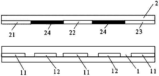
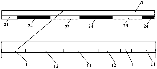
[0028] like image 3 and Figure 4 As shown, this embodiment provides an array substrate, including a plurality of sub-pixel units, and a light forming unit corresponding to each of the sub-pixel units for forming light of different colors is provided on the light-emitting surface side of the array substrate.
[0029] When the array substrate 1 and a color filter substrate 2 of this embodiment are used in a display device, each sub-pixel unit on the array substrate corresponds to a color filter on the color filter substrate, and each sub-pixel unit A pixel unit and its corresponding color filter form a sub-pixel. At this time, taking the backlight of the display device as an example that emits white light, the color filter substrate includes a red filter, a green filter, and a blue filter. The sub-pixel unit corresponding to the upper red filter is turned on, and the white light emitted by the backlight passes through the light forming unit corresponding to the sub-pixel uni...
Embodiment 2
[0039] This embodiment provides a method for preparing an array substrate. The array substrate may be the array substrate 1 described in Embodiment 1. The array substrate 1 includes a plurality of sub-pixel units. The method for preparing the array substrate includes:
[0040] Light forming units for forming light of different colors corresponding to each of the sub-pixel units are formed on the light emitting surface of the array substrate 1 .
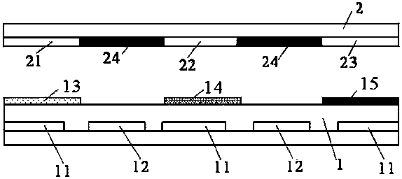
[0041] Preferably, the light forming unit includes: a red light forming unit, a green light forming unit, and a blue light forming unit, such as image 3 , 4 As shown, further preferably, the red light forming unit is a first quantum dot layer 13 composed of first quantum dots that can excite red light; the green light forming unit is a second quantum dot layer 13 that can excite green light. A second quantum dot layer 14 composed of quantum dots; the blue light forming unit is a third quantum dot layer 15 composed of third quantum d...
Embodiment 3
[0048] This embodiment provides a display device, which includes the array substrate 1 described in Embodiment 1, and a color filter substrate that is boxed with the array substrate, and the color filter substrate includes a plurality of color filters of different colors. A light sheet, wherein the color filters correspond to the sub-pixel units one by one, and the color of the light formed by the color filter corresponding to the sub-pixel units is the same as that of the light formed by the light forming unit.
[0049] The display device in this embodiment may also be any product or component with a display function such as a liquid crystal panel, electronic paper, liquid crystal TV, liquid crystal display, digital photo frame, mobile phone, and tablet computer.
[0050] The display device of this embodiment includes the array substrate described in Embodiment 1, so its display quality is higher.
PUM
| Property | Measurement | Unit |
|---|---|---|
| particle diameter | aaaaa | aaaaa |
| particle diameter | aaaaa | aaaaa |
| particle diameter | aaaaa | aaaaa |
Abstract
Description
Claims
Application Information
 - R&D
- Intellectual Property
- Life Sciences
- Materials
- Tech Scout
- Unparalleled Data Quality
- Higher Quality Content
- 60% Fewer Hallucinations
Browse by: Latest US Patents, China's latest patents, Technical Efficacy Thesaurus, Application Domain, Technology Topic, Popular Technical Reports.
© 2025 PatSnap. All rights reserved.Legal|Privacy policy|Modern Slavery Act Transparency Statement|Sitemap|About US| Contact US: help@patsnap.com