Pixel circuit and display device

A technology for pixel circuits and display devices, applied in static indicators, instruments, etc., can solve the problem of uneven display brightness of display devices, and achieve the effects of reducing the number of signal lines, reducing pixel spacing, and solving threshold voltage drift.

Active Publication Date: 2014-10-01
BOE TECH GRP CO LTD +1
View PDF6 Cites 8 Cited by
  • Summary
  • Abstract
  • Description
  • Claims
  • Application Information

AI Technical Summary

Problems solved by technology

[0006] The purpose of the present invention is to solve the problem of uneven display brightness of the display device, reduce the number of signal lines used for the pixel circuit in the display device, reduce the cost of the integrated circuit, and improve the pixel density of the display device at the same time

Method used


Image

  • Pixel circuit and display device
  • Pixel circuit and display device
  • Pixel circuit and display device

Examples


Embodiment 1

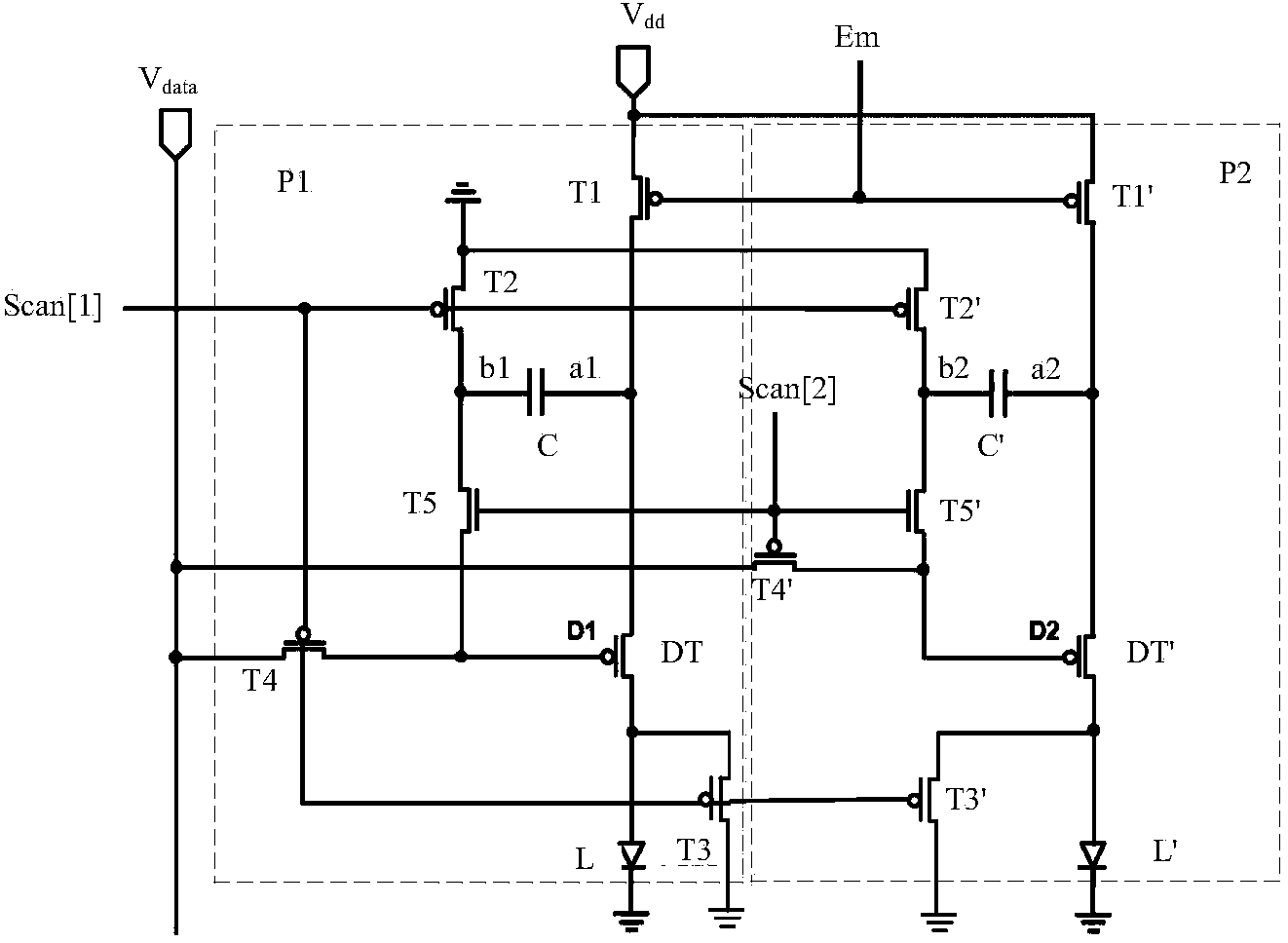
[0034] Embodiment 1 of the present invention provides a pixel circuit, such as figure 1 Or as shown in Figure 3, it includes: two sub-pixel circuits P1 and P2, where each sub-pixel circuit corresponds to a pixel; each pixel sub-circuit includes: five switching units T1, T2, T3, T4, T5, one driving unit DT, an energy storage unit C, and an electroluminescence unit L (for easy distinction, in figure 1 Or in Figure 3, the five switching units in P2 are represented as T1', T2', T3', T4', T5' respectively, the drive unit is represented as DT', the energy storage unit is C', and the electroluminescent unit is L ', the same below),

[0035] The similarities between the two sub-pixel circuits are (combined with P1 for explanation):

[0036] The control end of T1 is connected to the first scanning signal line Em, and the first end of T1 is connected to the working voltage line V dd , the second end of T1 is connected to the input end of DT, which is used to provide the working volta...

Embodiment 2

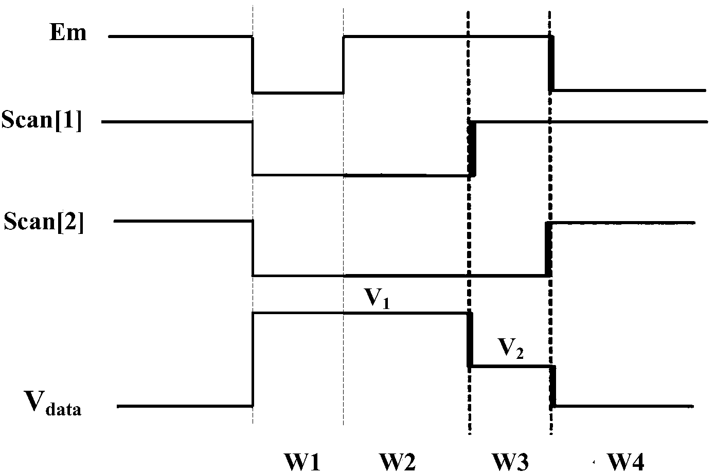
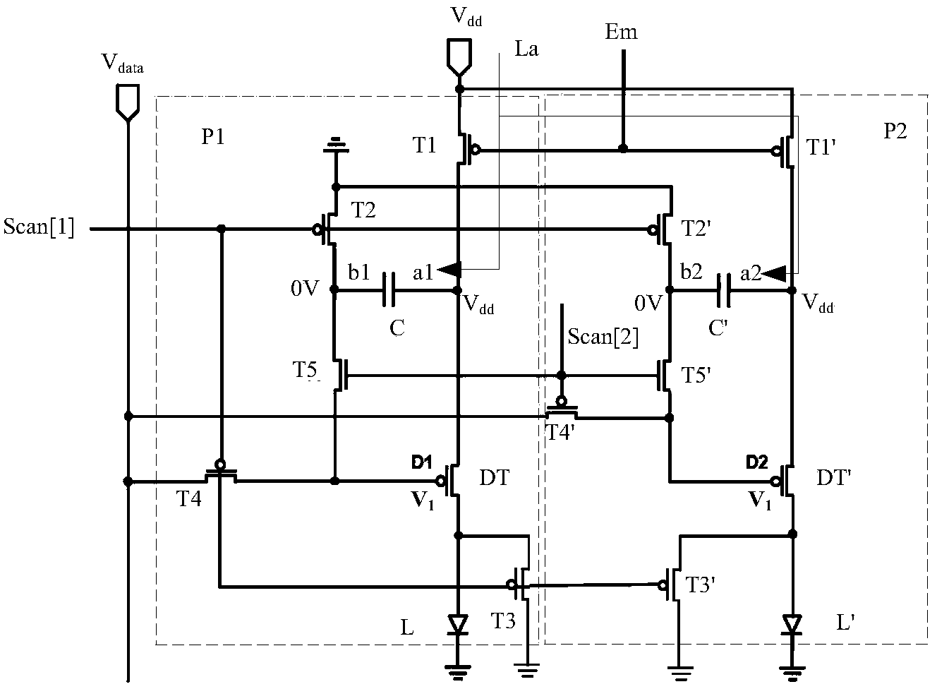
[0059] The difference between the pixel circuit provided by the second embodiment of the present invention and the pixel circuit provided by the embodiment is that the control terminal of T4' in P2 is connected to the fourth scanning signal Scan[3] (see Figure 4 ), the Scan[3] here is different from the above-mentioned Scan[2]. At this time, the channel type of T4' of P2 and the channel types of T5 and T5' can be the same or different. As long as the conduction state of T4' is reversed from the conduction state of T5 and T5' on the basis of the implementation of the first embodiment, the technical solution provided by the present invention can be realized, and its specific principle will not be described in detail here.

[0060] Preferably, the channel types of each switch unit and DT are the same. In this way, the manufacturing process of each switch unit and DT can be guaranteed to be consistent, and the manufacturing difficulty can be reduced.

[0061] preferred, such as ...


PUM


Abstract

The invention provides a pixel circuit and a display device. The pixel circuit comprises two sub-pixel circuits. Each sub-pixel circuit comprises five switch units, a driving unit, an energy storage unit and an electroluminescence unit. The two sub-pixel circuits share the same data voltage wire and multiple scanning signal lines. According to the pixel circuit, working currents flowing through devices of the electroluminescence unit can be free of influence of a threshold voltage of a corresponding driving transistor, and therefore the problem of non-uniform display brightness caused by drift of the threshold voltage of the driving transistor is thoroughly solved. Meanwhile, a compensating circuit is adopted for driving two pixels, and the two adjacent pixels share multiple signal lines, so the number of the signal lines used for the pixel circuit in the display device can be reduced, the cost of an integrated circuit is lowered, the pixel distance is shortened, and the pixel density is increased.

Description

technical field [0001] The present invention relates to the field of display technology, in particular to a pixel circuit and a display device. Background technique [0002] Organic light-emitting display (OLED) is one of the hot spots in the field of flat panel display research. Compared with liquid crystal display, OLED has the advantages of low energy consumption, low production cost, self-illumination, wide viewing angle and fast response speed. At present, OLEDs have begun to replace traditional liquid crystal (LCD) displays in display fields such as mobile phones, PDAs, and digital cameras. Pixel drive circuit design is the core technical content of OLED display, which has important research significance. [0003] Unlike TFT (Thin Film Field Effect Transistor)-LCD, which uses a stable voltage to control brightness, OLED is current-driven and requires a stable current to control light emission. [0004] Due to the process and device aging, in the original 2T1C driving...

Claims


Application Information

Patent Timeline
Patent Type & Authority Applications(China)
IPC IPC(8): G09G3/32G09G3/3208
CPCG09G3/32G09G3/3233
Inventor 杨盛际
Owner BOE TECH GRP CO LTD
Why Eureka
Try Eureka