

Semiconductor apparatus and methods for single-ended eDRAM sense amplifier
A semiconductor and device technology, applied in the direction of instruments, static memory, digital memory information, etc., can solve the problems of centering function loss, increased manufacturing cost, uncompetitive design, etc.
- Summary
- Abstract
- Description
- Claims
- Application Information
AI Technical Summary
Problems solved by technology
Method used
Image

Examples
Embodiment Construction
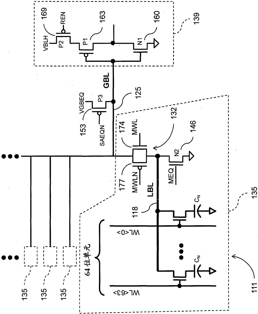
[0027] figure 1 A dynamic random access memory (DRAM) array having a segmented bit line structure, generally designated 111, is shown. figure 1 The structures shown are examples only, and those skilled in the art will understand that the systems and methods described herein may be used with figure 1 Similar arbitrary structures are applied and used together.
[0028] In this example, DRAM array 111 includes multiple DRAM cells integrated on the same die arranged along 64 word lines (WL-WL). As used herein, for embedded DRAM, a DRAM cell may be referred to as eDRAM. Each group of 64-bit cells of DRAM array 111 is connected to a local bit line 118, sometimes referred to herein as an LBL. LBL 118 is coupled to global bit line 125 , sometimes referred to herein as a GBL, through multiplexer device 132 . According to the systems and methods herein, multiplexer device 132 may comprise a CMOS multiplexer.
[0029] For convenience, LBL 118 , group of 64-bit cells, and multiplexer...
PUM
 Abstract
Description
Claims
Application Information