Method for forming self-aligned triple graphs

A self-alignment and graphics technology, applied in the direction of electrical components, semiconductor/solid-state device manufacturing, circuits, etc., can solve the problems of process limitations, single application of self-alignment double pattern masks, and inability to adapt to technical requirements, etc., to reduce costs , The effect of simple process

Active Publication Date: 2014-10-01
SEMICON MFG INT (SHANGHAI) CORP
View PDF6 Cites 6 Cited by
  • Summary
  • Abstract
  • Description
  • Claims
  • Application Information

AI Technical Summary

Problems solved by technology

[0009] However, the size of the self-aligned double pattern mask formed by the prior art is still limited by the process...

Method used


Image

  • Method for forming self-aligned triple graphs
  • Method for forming self-aligned triple graphs
  • Method for forming self-aligned triple graphs

Examples


Embodiment Construction

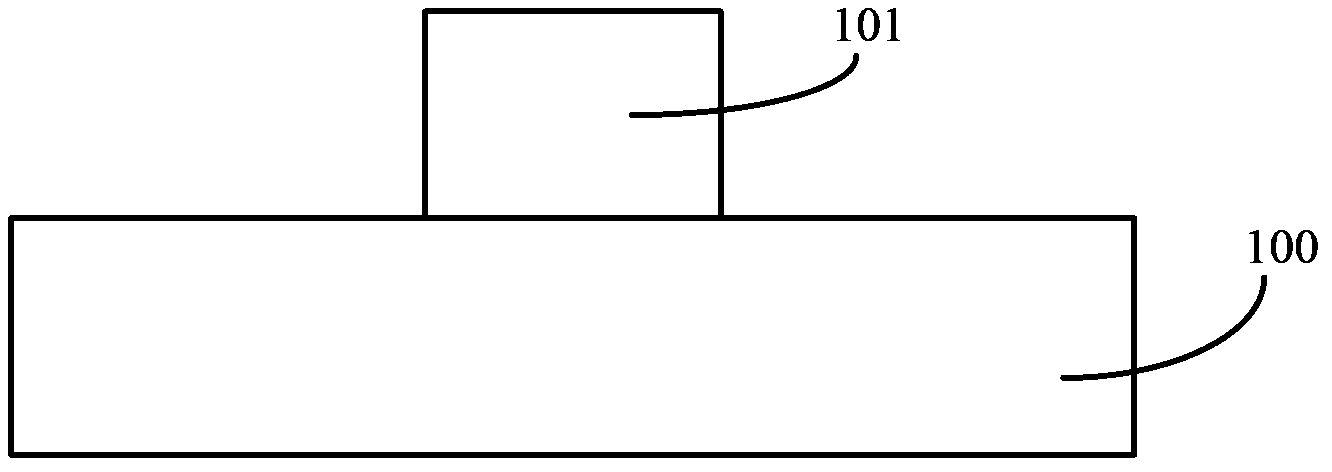
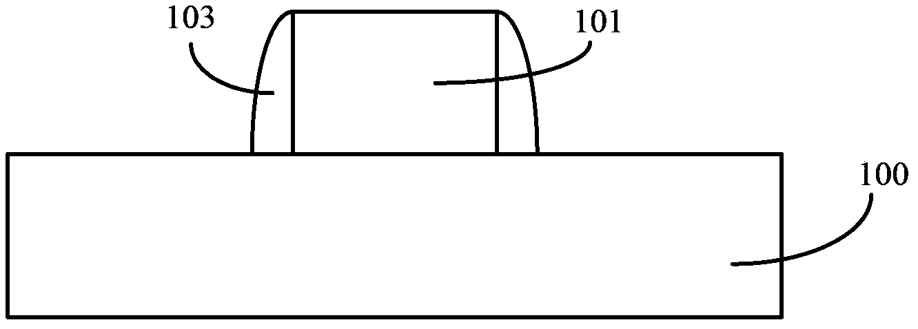
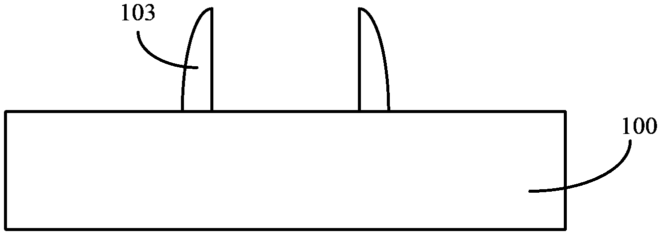
[0037] As mentioned in the background, the size of the self-aligned double pattern mask formed in the prior art cannot be further reduced.

[0038] The inventor of the present invention has found through research, please continue to refer to Figure 1 to Figure 3 , in the prior art, mask spacers 103 are respectively formed on both sides of the sacrificial layer 101 by using a self-alignment process (that is, a deposition process and an etch-back process after the deposition process), and only a single sacrificial layer can be formed A double number of mask spacers 103 can be formed within the range of 101 . However, the size of the sacrificial layer 101 cannot be further reduced due to the limitation of the accuracy of the existing photolithography process, which limits the reduction of the distance between adjacent mask spacers 103, and the size of the formed mask spacer 103 All are the same, so that the mask sidewall 103 cannot meet the requirements of more miniaturized and ...


PUM

PropertyMeasurementUnit
Thicknessaaaaaaaaaa

Abstract

A method for forming self-aligned triple graphs comprises the steps of providing a to-be-etched layer, wherein part of the surface of the to-be-etched layer is provided with a plurality of split first sacrificial layers, the surface of the to-be-etched layer is exposed between the adjacent first sacrificial layers, and the surfaces of the first sacrificial layers are provided with second sacrificial layers; forming mask films on the surface of the to-be-etched layer, the surfaces of the first sacrificial layers and the surfaces of the second sacrificial layers; removing the mask films on side walls and top surfaces of the second sacrificial layers and forming first masks on two sides of the first sacrificial layers; after the first masks are formed, removing part of the second sacrificial layers along side wall surfaces of the second sacrificial layers to reduce the dimensions of the second sacrificial layers and expose part of the surfaces of the first sacrificial layers, and reducing the dimensions until the second sacrificial layers form second masks. The method is simple, and the formed triple graphs are applied more widely.

Description

technical field [0001] The invention relates to the technical field of semiconductor manufacturing, in particular to a method for forming a self-aligned triple pattern. Background technique [0002] With the continuous progress of semiconductor technology, the process nodes of semiconductor devices are continuously reduced. However, due to the limitation of the precision of the existing photolithography process, the mask pattern formed by the existing photolithography process is difficult to meet the demand for continuous reduction of the feature size of semiconductor devices, which hinders the development of semiconductor technology. [0003] In order to further reduce the size of the semiconductor device on the basis of the existing photolithography process, a double patterning process is proposed in the prior art. Among them, a self-aligned double patterning (Self-Aligned Double Patterning, SADP) process is widely used because of its simple process. [0004] Figure 1 t...

Claims


Application Information

Patent Timeline
IPC IPC(8): H01L21/033H01L21/02H01L21/308
CPCH01L21/0338
Inventor 尚飞何其旸
Owner SEMICON MFG INT (SHANGHAI) CORP
Why Eureka
Try Eureka