Bonding alignment mark and method for calculating offset

An alignment mark and offset technology, applied in semiconductor/solid-state device testing/measurement, electrical components, electrical solid-state devices, etc., can solve the problems of poor control of the bonding process and results, and improve production quality and quality. rate effect

Active Publication Date: 2014-10-01
SEMICON MFG INT (SHANGHAI) CORP
View PDF3 Cites 24 Cited by
  • Summary
  • Abstract
  • Description
  • Claims
  • Application Information

AI Technical Summary

Problems solved by technology

[0007] The purpose of the present invention is to provide a bonding alignment mark and a method for calculating the offset to solve the problem of poor control of the bonding process and results in the prior art

Method used


Image

  • Bonding alignment mark and method for calculating offset
  • Bonding alignment mark and method for calculating offset
  • Bonding alignment mark and method for calculating offset

Examples


Embodiment Construction

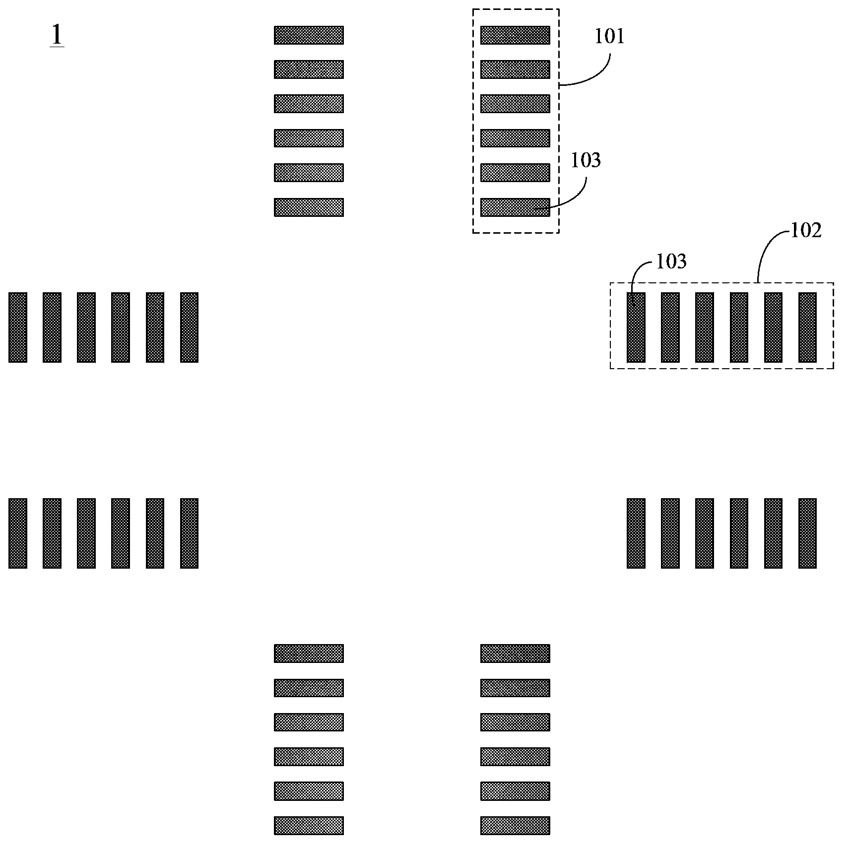
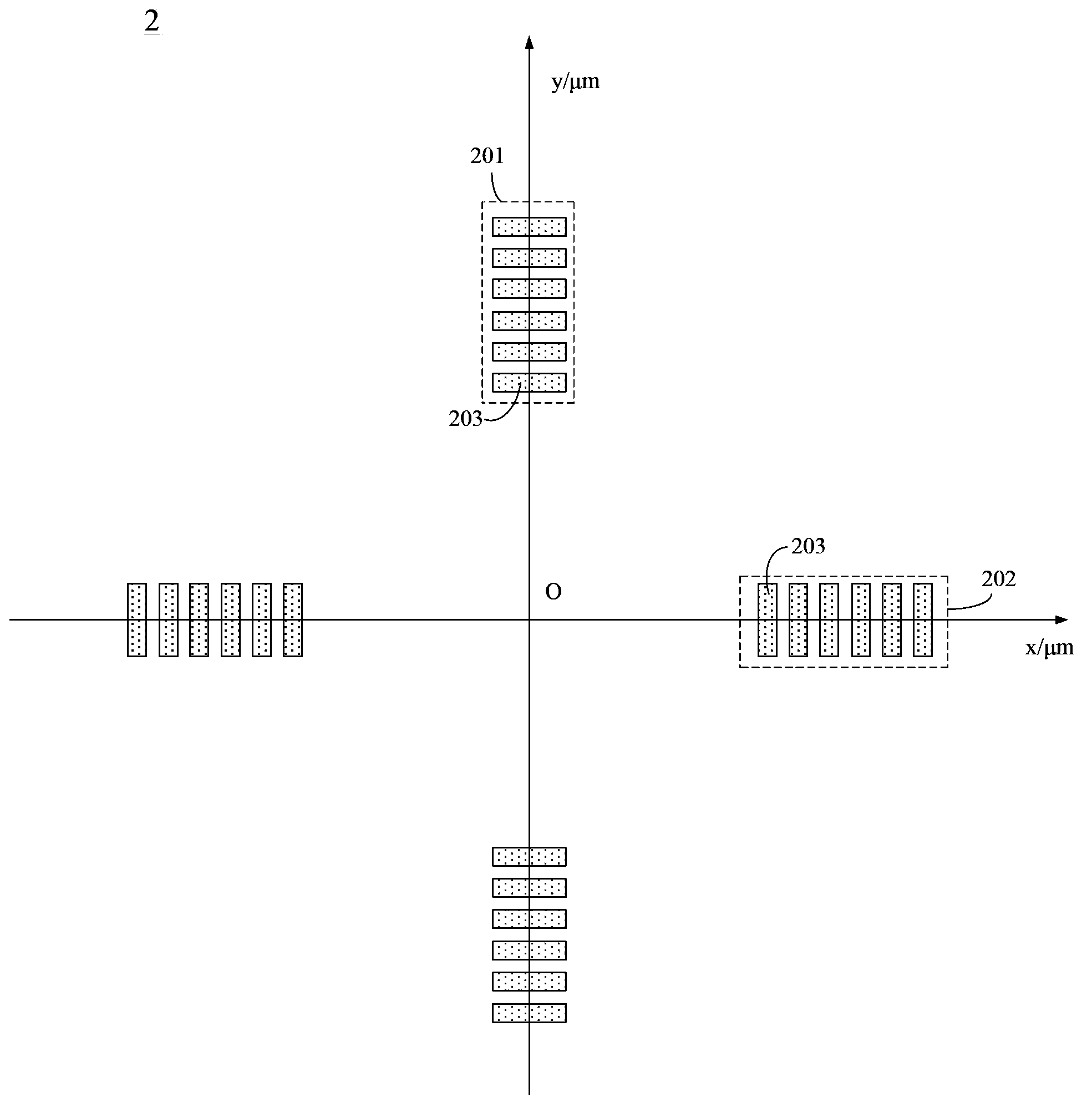
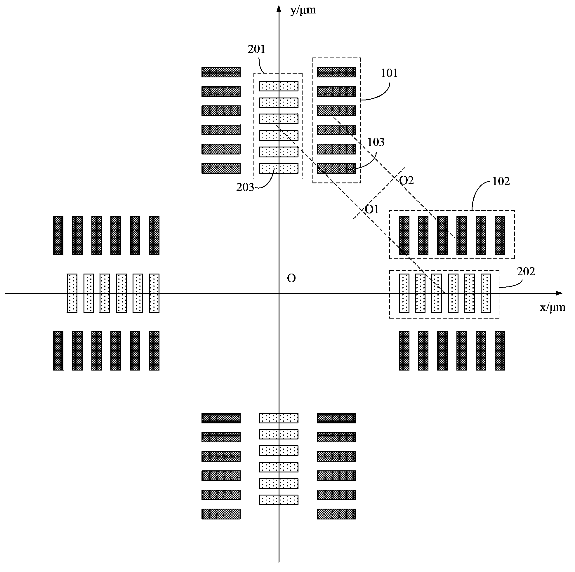
[0031] It has been mentioned in the background that at present, due to the shortage of equipment involved in the bonding process, silicon wafers are prone to large deviations during bonding. After long-term experiments, the inventors found that by making full use of existing resources and forming alignment marks with a specific structure on the silicon wafers to be bonded, the deviation of the silicon wafers can be reduced as much as possible.

[0032] The bonding alignment mark and the method for calculating the offset provided by the present invention will be further described in detail below with reference to the drawings and specific embodiments. Advantages and features of the present invention will be apparent from the following description and claims. It should be noted that all the drawings are in a very simplified form, and are only used for the purpose of conveniently and clearly assisting in describing the embodiments of the present invention.

[0033] First please ...


PUM


Abstract

The invention discloses a bonding alignment mark and a method for calculating offset. A first alignment mark is arranged on a first silicon wafer; a second alignment mark is arranged on a second silicon wafer; each of the first alignment mark and the second alignment mark comprises a plurality of transverse marks and longitudinal marks; each of the transverse marks and the longitudinal marks comprises a plurality of uniformly distributed alignment scales; and spacings of the adjacent alignment scales in the first alignment mark are different from spacings of the adjacent alignment scales in the second alignment mark. Therefore, when the two silicon wafers are bonded, the offset of the two silicon wafers in a bonding process can be obtained, and the offset can be obtained precisely by obtaining the quantity of the alignment scales before the aligned same-order alignment scales and combining the spacings of the alignment scales; technical personnel can timely handle; the production quality is improved; and the yield is increased.

Description

technical field [0001] The invention relates to the field of semiconductor manufacturing, in particular to a bonding alignment mark and a method for calculating an offset. Background technique [0002] In recent years, with the continuous progress of semiconductor technology, various new technologies have been continuously developed. At present, the manufacture of devices is not satisfied with only forming on a single silicon wafer, but combining multiple silicon wafers together. The model has been approved. [0003] For the production process of this mode, silicon-silicon direct bonding and silicon-glass electrostatic bonding technologies are commonly used. Recently, a variety of new bonding technologies have been developed, such as metal-metal bonding technology. [0004] At present, for metal-to-metal bonding, bonding offset is a common problem in the industry. If the bonding offset is large, it will affect the quality of the bonding. Some devices have strict requirement...

Claims


Application Information

Patent Timeline
Patent Type & Authority Applications(China)
IPC IPC(8): H01L23/544H01L21/66
Inventor 黄平郭亮良
Owner SEMICON MFG INT (SHANGHAI) CORP
Why Eureka
Try Eureka