Electrostatic protection structure and electrostatic protection circuit

A technology for electrostatic protection and power supply, applied in circuits, electrical components, electric solid devices, etc., can solve the problem of low discharge efficiency of ESD protection circuits, and achieve the effect of improving efficiency and strengthening control capabilities.

Active Publication Date: 2014-10-01
SEMICON MFG INT (SHANGHAI) CORP
View PDF3 Cites 15 Cited by
  • Summary
  • Abstract
  • Description
  • Claims
  • Application Information

AI Technical Summary

Problems solved by technology

[0006] Existing ESD protection circuits have low discharge efficiency when discharging

Method used


Image

  • Electrostatic protection structure and electrostatic protection circuit
  • Electrostatic protection structure and electrostatic protection circuit
  • Electrostatic protection structure and electrostatic protection circuit

Examples


Embodiment Construction

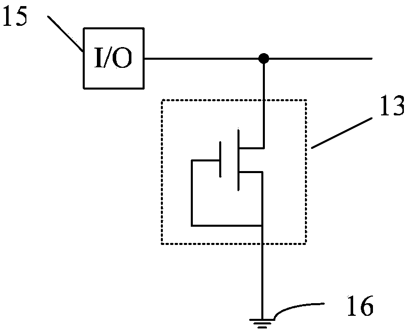
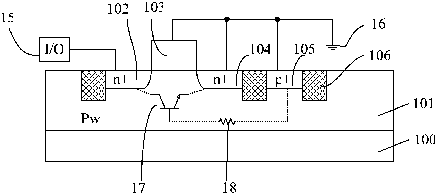
[0034] The existing electrostatic protection circuit passes the parasitic NPN triode 17 (refer to figure 2 ) discharge, there is only one discharge path, and when the parasitic NPN transistor is turned on and discharged, it is passively triggered, that is, when the electrostatic charge accumulates a certain amount of electrostatic charge at the input and output interface terminal 15, the current flows from the drain region 102 through the well region resistance 18 to The P-type doped region 105 region makes a potential difference between the P well region at the bottom of the gate 103 and the ground terminal 16. When the potential difference is greater than the threshold voltage of the parasitic NPN transistor 17, the electrostatic charge accumulated at the input and output interface terminal 15 is released. The efficiency of electrostatic discharge of the existing electrostatic protection circuit is relatively low.

[0035] In order to solve the above problems, the present i...


PUM


Abstract

The invention provides an electrostatic protection structure and an electrostatic protection circuit. The electrostatic protection structure comprises a PMOS transistor located in a first region of a first N-type trap, a first base doping region located in a second region of the first N-type trap, an NMOS transistor located in a third region of a first P-type trap and a second base doping region located in a fourth region of the first P-type trap. The source region and grid electrode of the PMOS transistor are connected with a power supply end. The drain region of the PMOS transistor is connected with an input / output interface end. The first base doping region is connected with an external trigger voltage regulator circuit. The drain region of the NMOS transistor is connected with the input / output interface end. The grid electrode and source region of the NMOS transistor are connected with a grounding end. The second base doping region is connected with the external trigger voltage regulator circuit. According to the electrostatic protection structure and the electrostatic protection circuit, paths of electrostatic discharge of the electrostatic protection structure are increased, and electrostatic discharge efficiency is improved.

Description

technical field [0001] The invention relates to the field of electrostatic protection, in particular to an electrostatic protection structure and an electrostatic protection circuit. Background technique [0002] In the production and application of integrated circuit chips, with the continuous improvement of VLSI process technology, the current CMOS integrated circuit production technology has entered the deep submicron stage, the size of MOS devices is continuously shrinking, and the thickness of the gate oxide layer is increasing. The thinner the MOS device is, the lower the withstand voltage capability of the MOS device is, and the harm of electrostatic discharge (ESD) to integrated circuits becomes more and more significant. Therefore, it becomes particularly important to protect integrated circuits from ESD. [0003] In order to strengthen the ability to protect against static electricity, most of the chip's input and output interface (I / O pad) is connected to an elec...

Claims


Application Information

Patent Timeline
Patent Type & Authority Applications(China)
IPC IPC(8): H01L27/02
Inventor 欧阳雄翁文君程惠娟陈捷李宏伟
Owner SEMICON MFG INT (SHANGHAI) CORP
Why Eureka
Try Eureka