Optical device measurement method and measurement device based on double sideband modulation

A measuring device and double-sided band technology, which is applied in the direction of testing optical properties, etc., can solve problems such as inconvenient adjustment, limited extinction ratio, and complex system, and achieve the effects of improving system stability, eliminating limited extinction ratio, and reducing system complexity

Active Publication Date: 2016-08-17
NANJING UNIV OF AERONAUTICS & ASTRONAUTICS
View PDF7 Cites 0 Cited by
  • Summary
  • Abstract
  • Description
  • Claims
  • Application Information

AI Technical Summary

Problems solved by technology

[0004] However, the measurement method of optical devices based on SSB modulation also has serious deficiencies
First of all, the generation of optical SSB will make the system very complicated. The current SSB generation methods are roughly divided into filtering method and 90° phase shift method. The former requires the use of filters, which increases the complexity and instability of the system, and The extinction ratio is limited; the latter requires a 90° phase shift of the microwave signal loaded to the dual-drive optoelectronic modulator, requiring the use of a broadband 90° bridge and a dual-drive optoelectronic modulator, the system is complex and inconvenient to adjust
Secondly, the SSB frequency sweep method can only obtain a set of measurement signals in one measurement, and the measurement efficiency is low.
Finally, the SSB sweep method is severely limited by the instrumentation, e.g. the SSB sweep range cannot be larger than the photodetector (PD) bandwidth

Method used


Image

  • Optical device measurement method and measurement device based on double sideband modulation
  • Optical device measurement method and measurement device based on double sideband modulation
  • Optical device measurement method and measurement device based on double sideband modulation

Examples


Embodiment Construction

[0021] The technical scheme of the present invention is described in detail below in conjunction with accompanying drawing:
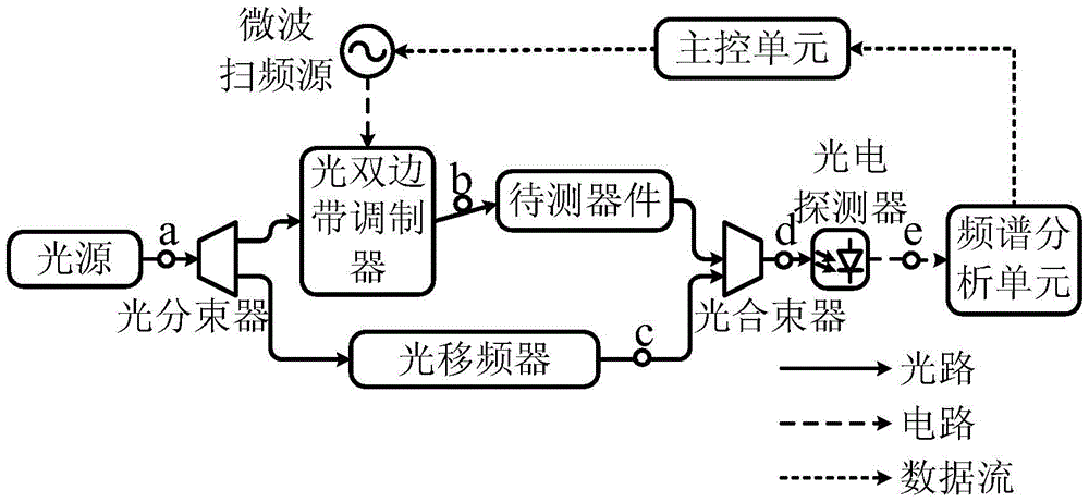
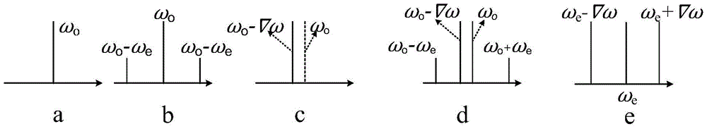
[0022] The idea of ​​the present invention is to add an optical carrier that is coherent with the original optical carrier and has a small frequency difference to the optical double sideband modulation signal passing through the device under test, so that after the photodetector beats, the microwave components corresponding to the ±1st order sideband With different frequencies, the magnitude response information on the ±1st order sidebands can be extracted simultaneously.

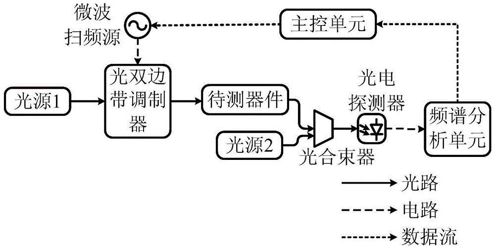
[0023] figure 1 An embodiment of the optical device measuring device of the present invention is shown, as figure 1 As shown, the device includes a light source, an optical beam splitter, an optical beam combiner, an optical frequency shifter, an optical double sideband modulator, a microwave frequency sweep source, a photodetector, a spectrum analysis unit, and a main control unit....


PUM


Abstract

The invention discloses an optical device measurement method based on double sideband modulation, and belongs to the technical fields of optical device measurement and microwave photonics. First, the radio frequency signal is modulated on the first optical carrier signal by using the optical double sideband modulation method to generate a double sideband modulation signal; then the double sideband modulation signal is combined with the second optical carrier signal after passing through the optical device to be tested, and the second There is a frequency difference between the optical carrier signal and the first optical carrier signal; use a photodetector to beat the combined signal, and then extract the amplitude of the +1-order sideband signal and the -1-order sideband signal in the beat frequency signal Information; scanning the frequency of the radio frequency signal, that is, obtaining the wideband amplitude-frequency response of the optical device to be tested. The invention also discloses an optical device measurement device based on double sideband modulation. The invention greatly improves the measurement range and measurement efficiency while reducing the complexity and cost of the system, and more importantly, opens up a new direction for the optical device measurement technology.

Description

technical field [0001] The invention relates to an optical device measurement method, in particular to an optical device measurement method and a measurement device based on double sideband modulation, and belongs to the technical fields of optical device measurement and microwave photonics. Background technique [0002] In recent years, with the rapid development of laser technology, photonic systems have been widely used, such as ultra-high-precision optical fiber sensing, long-distance optical fiber communication, etc. However, the development of optical measurement technology has stagnated, which not only makes it difficult to develop and manufacture high-precision optical devices, but also makes it impossible for existing optical devices to maximize their effectiveness in optical systems. For example: the minimum bandwidth of Fiber Bragg Grating (FBG) is as low as 9MHz, while the measurement accuracy of existing optical measurement technology is still hundreds of MHz (c...

Claims


Application Information

Patent Timeline
Patent Type & Authority Patents(China)
IPC IPC(8): G01M11/02
Inventor 潘时龙卿婷薛敏黄梦昊
Owner NANJING UNIV OF AERONAUTICS & ASTRONAUTICS
Why Eureka
Try Eureka