
Color film substrate, liquid crystal module and touch display device

A color film substrate and liquid crystal module technology, which is applied in optics, instruments, electrical digital data processing, etc., can solve the problems of unable to monitor FPC binding status, blind binding, and detection of FPC binding status, so as to improve the process quality Yield, avoiding quality accidents, and reducing the effect of accidents

Active Publication Date: 2014-10-15
BOE TECH GRP CO LTD +1
View PDF4 Cites 13 Cited by
  • Summary
  • Abstract
  • Description
  • Claims
  • Application Information

AI Technical Summary

Problems solved by technology

In the conventional liquid crystal module, there is such a problem in the touch flexible printed circuit (Touch Flexible Printed Circuit, TFPC) bonding technology link: the plug-in touch technology binds the touch flexible printed circuit to the color film substrate The upper layer of the FPC, while ordinary microscopes cannot penetrate the FPC and gold fingers to detect the binding state of the FPC. Under the infrared light microscope, the dislocation can only be barely observed, and the conductive particles cannot be detected.
Therefore, in the existing Touch FPC binding technology link, the upper layer is the FPC and the lower layer is the BM area structure, which makes it impossible to monitor the FPC binding status on both sides
Production without detection and monitoring will cause the process quality of the Touch FPC binding link to be unable to be guaranteed, resulting in a blind binding state, which is very risky, and once a binding problem occurs, the loss will be serious

Method used


Image

  • Color film substrate, liquid crystal module and touch display device
  • Color film substrate, liquid crystal module and touch display device

Examples


no. 1 example

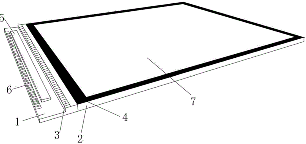
[0020] Such as figure 1 As shown, according to the first embodiment of the present invention, a color filter substrate 2 is provided, and the color filter substrate 2 includes a flexible printed circuit (TFPC) binding area 3 for touch control and a black matrix BM area 4 .

[0021] Wherein, the TFPC binding area 3 is used for binding the flexible printed circuit for touch control, and its bottom is transparent, while the BM area 4 is used for light shielding.

[0022] Wherein, the TFPC binding area 3 and the BM area 4 are two mutually independent areas, and the two areas have no overlapping area or a partial overlapping area; and, the bottom of the flexible printed circuit binding area for touch is transparently set .

[0023] Specifically, the color filter substrate 2 may be a glass substrate, and the bottom of the TFPC binding region 3 may be transparent glass.

[0024] In fact, it is equivalent to increasing the length of the original color filter glass substrate, and the...


PUM


Abstract

The invention relates to the technical field of displaying, in particular to a color film substrate, a liquid crystal module and a touch display device. The color film substrate comprises a touch flexible printed circuit binding area and a black matrix area; the touch flexible printed circuit binding area is used for binding a touch flexible printed circuit; the black matrix area is used for shading the light; the touch flexible printed circuit binding area and the black matrix area are two mutually independent areas; the two areas are never superposed or partially superposed; the bottom of the touch flexible printed circuit binding area is transparent. The externally-hung touch structure is re-designed; the bottom of the TFPC (touch flexible printed circuit) is in a glass transparent state, with no BM (black matrix) shading; and accordingly TFPC binding state and conducting particle state can be monitored from the back with a common microscope, yield of the externally-hung TFOG (touch FPC on glass) process is greatly increased, original uncontrollable production is turned into monitorable production, accident rate is greatly reduced, and unnecessary quality accidents are avoided.

Description

technical field [0001] The invention relates to the field of display technology, in particular to a color filter substrate, a liquid crystal module module and a touch display device. Background technique [0002] At present, the touch on cell (Touch on cell) technology is gradually popularized. The main method is to embed the touch screen between the color filter substrate and the polarizer of the display screen, that is, to equip the touch sensor on the liquid crystal panel. In the existing display technology, a conventional liquid crystal module includes an upper polarizer, a color filter substrate (including a black matrix BM (light-shielding area)), a liquid crystal, an array substrate, a lower polarizer, and a backlight module (including a BM area ). In the conventional liquid crystal module, there is such a problem in the touch flexible printed circuit (Touch Flexible Printed Circuit, TFPC) bonding technology link: the plug-in touch technology binds the touch flexible...

Claims


Application Information

Patent Timeline
IPC IPC(8): G06F3/041G02F1/1333
CPCG02F1/133305G02F1/13338G02F1/133512G06F3/0412G06F3/04164G02F1/133388G02F1/133514G02F1/133528G06F3/041G06F2203/04102G06F2203/04103
Inventor 王大鹏
Owner BOE TECH GRP CO LTD
Learn More