

Device for nondestructively detecting resistivity of silicon wafer by terahertz and application method of device
A non-destructive testing and terahertz detector technology, applied in the terahertz field, can solve problems such as many equipment links, unsuitable silicon wafer sample census, complex circuit design, etc., and achieve the effect of improving yield and quality
- Summary
- Abstract
- Description
- Claims
- Application Information
AI Technical Summary
Problems solved by technology
Method used
Image

Examples
Embodiment 1
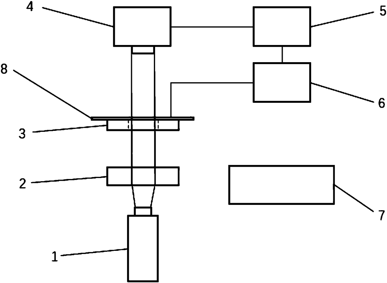
[0024] Such as figure 1 As shown, a terahertz non-destructive testing device for the resistivity of a silicon wafer includes a terahertz radiation source 1, a collimated beam expander system 2, at least one parallel movable sample stage 3, a terahertz detector 4, a computer 5, and a Mechanical suction cups 6 for grabbing silicon wafers, reworked wafer collection boxes 7. The terahertz radiation source 1 is preferably a terahertz quantum cascade laser with a frequency of 4.3 THz, which is arranged at the bottom of the device and radiates terahertz waves vertically upward. The collimated beam expander system 2 is preferably a Galileo type collimated beam expander system, which is arranged above the terahertz radiation source 1 . The sample stage 3 is preferably a sample stage with an aperture of 3 cm that can move horizontally in one direction, and the number is multiple, and it is arranged above the collimator beam expander system 2 . The terahertz detector 4 is preferably a ...
PUM
| Property | Measurement | Unit |
|---|---|---|
| Diameter | aaaaa | aaaaa |
| Diameter | aaaaa | aaaaa |
| Side length | aaaaa | aaaaa |
Abstract
Description
Claims
Application Information