

PCB BGA area zero-distance through hole design method
A design method and zero-distance technology, applied in the directions of printed circuit components, electrical connection printed components, electrical components, etc., can solve the problems of high cost of resin plug holes, low application degree, yellow false copper exposure, etc. The effect of yield and quality, strong practicability, and wide application
- Summary
- Abstract
- Description
- Claims
- Application Information
AI Technical Summary
Problems solved by technology
Method used
Image

Examples
Embodiment 1
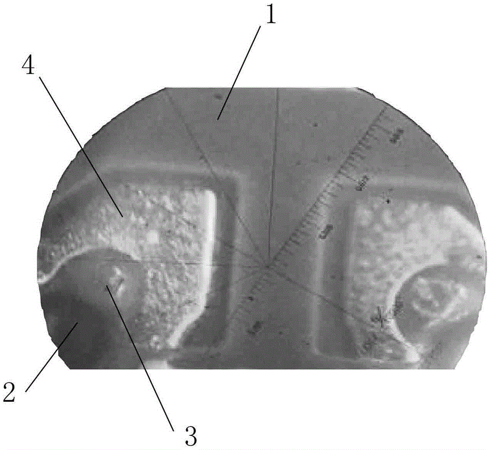
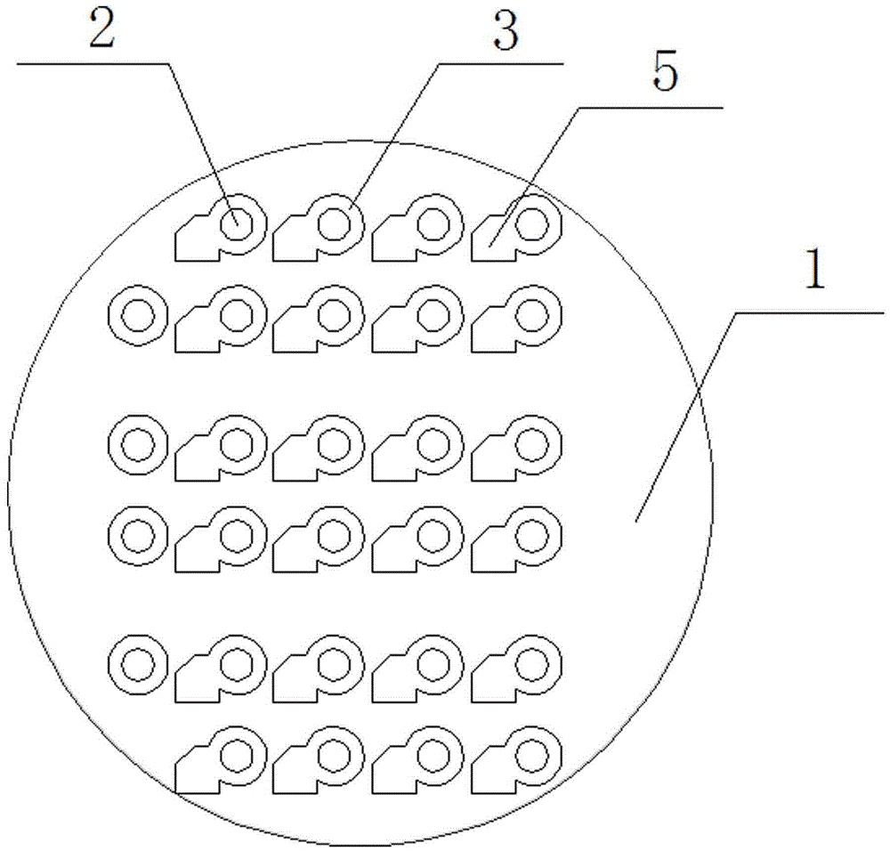
[0023] In the BGA area where the spherical contacts of the PCB board are displayed, several via holes are opened as required, and a pad is arranged outside the via hole. The pad is offset by a certain distance from the via hole, and an oil cover ring is set within the offset distance. The oil cover ring is a concave ring surrounding the outer side of the via hole, and the outer side of the oil cover ring is in contact with the edge of the pad.
[0024] The distance between the via hole and the pad is 3mil, that is, the ring diameter of the oil cover ring is 3mil.
[0025] After the cover oil ring is opened, ink plugging is carried out through the hole, and the ink plugging hole is cured in sections at 65°C×90min+85°C×150min+100°C×60min+120°C×40min+150°C×60min.
[0026] The via holes in the PCBBGA area directly use ink plug holes, especially when there are many layers and the PCB board is thick. This patent corrects the original design of the connection part between the via ho...
Embodiment 2
[0029] The ring diameter distance of the oil cover ring between the via hole and the pad is designed to be 4mil, and the other steps are the same as in the first embodiment.
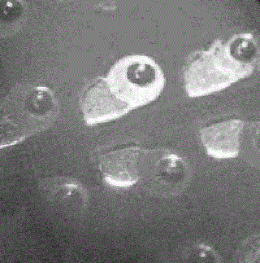
[0030] Since the ink flow between the via hole and the pad can reach up to 4mil, the ring diameter of the oil cover ring is expanded to 4mil here to ensure that the ink plug hole is continued to be used during the PCB manufacturing process, and the via hole in the BGA area appears Oozing explosive oil, if attached image 3 As shown, the presence of the added oil cover ring will also block the explosive oil, so that the explosive oil cannot flow to the pad, ensuring that the pad is clean and pollution-free, thereby effectively preventing poor soldering of the pad.
[0031] After using the design of the present invention, when the inspection is performed again, there is no phenomenon of oil explosion on the pad, and the use effect is ideal; the test verification shows that the problem of PCBBGA via hole ex...
PUM
 Abstract
Description
Claims
Application Information