Multi-substrate three-dimensional chip packaging method

A three-dimensional packaging and multi-substrate technology, which is applied in semiconductor/solid-state device manufacturing, electrical components, circuits, etc., can solve problems that cannot satisfy users, violate the original intention of design, and cannot meet wiring requirements, etc., and achieve the elimination of peripheral circuits and components. device, reduce design difficulty and cost, and improve the effect of signal integrity

Inactive Publication Date: 2014-10-15
NO 8357 RES INST OF THE THIRD ACADEMY OF CHINA AEROSPACE SCI & IND
View PDF2 Cites 2 Cited by
  • Summary
  • Abstract
  • Description
  • Claims
  • Application Information

AI Technical Summary

Problems solved by technology

[0004] In the design process of the system chip, designers often encounter the situation that the substrate area cannot meet the design requirements, that is, the total area of ​​the bare chip is larger than the substrate area or the layout cannot meet the wiring requirements
In this case, designers often can only make a compromise by expanding the chip area or cutting system functions. However, such processing methods are contrary to the original intention of the design, and cannot even meet the requirements of users.

Method used


Image

  • Multi-substrate three-dimensional chip packaging method
  • Multi-substrate three-dimensional chip packaging method
  • Multi-substrate three-dimensional chip packaging method

Examples


Embodiment 1

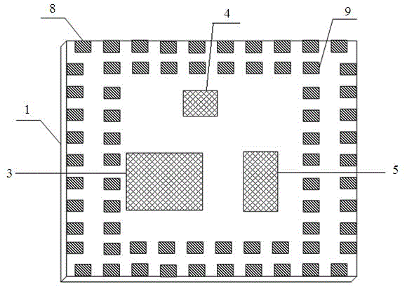
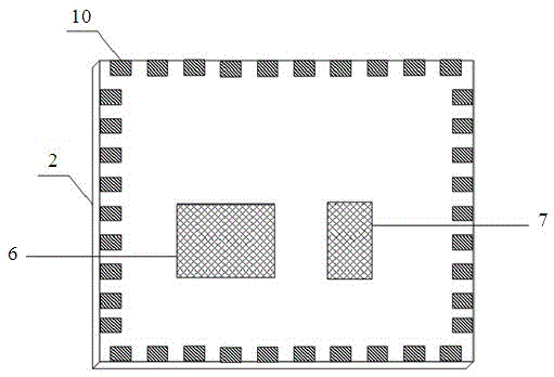
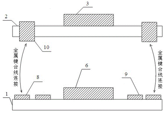
[0034] This embodiment designs a three-dimensional package chip with two substrates (see Figure 1-3 ), the chip substrate includes a main substrate 1, a sub-substrate 2, a first bare chip 3, a second bare chip 4, a third bare chip 5, a fourth bare chip 6 and a fifth bare chip 7; the main substrate 1 is close to There are two circles of PAD points around the edge, namely the outer circle PAD point 8 and the inner circle PAD point 9; the first bare chip 3, the second bare chip 4, and the third bare chip 5 are respectively installed on the main substrate 1, It is connected with the inner ring PAD point 9 through the printed wire; the fourth bare chip 6 and the fifth bare chip 7 are respectively installed on the sub-substrate 2; the edge of the sub-substrate 2 has a circle of PAD points 10, the fourth The signals to be drawn from the bare chip 6 and the fifth bare chip 7 are connected to the PAD point 10 through the printed wire. The signal to be drawn is connected to the outer ...


PUM


Abstract

The invention discloses a multi-substrate three-dimensional chip packaging method which is characterized by comprising the steps of integrating and interconnecting a plurality of organic substrates in a chip package, allowing the organic substrates to interconnect bare chips in a plane interconnection manner or a three-dimensional stacking manner, interconnecting the substrates by metal bonding wires, and forming a three-dimensional multi-substrate system chip. The method solves the problem of inadequate wiring resource of a single-substrate system chip, can provides an adequate wiring resource for design of the whole chip, can achieve most functions of a whole system with the single chip, saves a large number of peripheral circuits and components, reduces the design difficulty of the system, and improves the signal integrity of the system.

Description

technical field [0001] The invention belongs to the technical field of system chip design and packaging, in particular to a multi-substrate three-dimensional packaging chip method. According to the function and structure division of the bare chips, the method integrates the bare chips on multiple organic substrates, designs and packages them in a three-dimensional stacking manner, and forms a multi-substrate SiP (system-in-package) chip. Background technique [0002] With the rapid development of the integrated circuit industry, the feature size of chips is getting smaller and smaller, the scale of integration is getting larger and larger, and the functions realized are becoming more and more complex. They are widely used in various industries and become an indispensable part of human life. . However, due to the complex functions of the chip system and the increasingly high requirements for system integration in the industry, the traditional mode of integrating each chip at...

Claims


Application Information

Patent Timeline
IPC IPC(8): H01L21/58H01L21/60
CPCH01L21/768
Inventor 李鑫朱天成杨阳
Owner NO 8357 RES INST OF THE THIRD ACADEMY OF CHINA AEROSPACE SCI & IND
Why Eureka
Try Eureka