Circuit board and thermal printing head using same

A thermal printing head, circuit substrate technology, applied in the direction of printed circuit, printed circuit manufacturing, printed circuit components, etc., can solve the problems of wire bonding strength (low tensile strength, reliability cannot be ensured, etc., without reducing the lead wire Effects of joint strength, reduction of unit consumption, and reduction of power costs for firing furnaces

Inactive Publication Date: 2014-10-15
AOI ELECTRONICS CO LTD
View PDF5 Cites 5 Cited by
  • Summary
  • Abstract
  • Description
  • Claims
  • Application Information

AI Technical Summary

Problems solved by technology

However, in this case, the wire bonding strength (tensile strength) of the gold wire bonding portion 6 is low, and reliability cannot be ensured.

Method used


Image

  • Circuit board and thermal printing head using same
  • Circuit board and thermal printing head using same
  • Circuit board and thermal printing head using same

Examples


Embodiment 1

[0068] In this example, 22K gold (composition: organic gold) was used as the low-purity gold layer, and 24K gold (composition: organic gold) was used as the high-purity gold layer to prepare and test three samples.

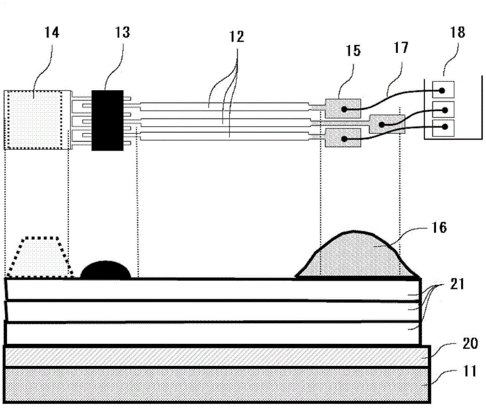
[0069] Make Figure 7 Sample of the configuration shown.

Embodiment 2

[0078] Comparing the hot spots through the above three samples ( figure 2 Of 13) Impulse resistance.

[0079] The test method is described below. Show the test results in Figure 4 .

[0080] Figure 4 Indicates at the wire bonding part ( figure 2 Of 15) with the common electrode ( figure 2 The correlation between the voltage when the pulse voltage is applied (pulse voltage) and the resistance value of the heating point between 14). From this test result, it is judged that it is not inferior to Comparative Example 1 (conventional) in pulse resistance.

Embodiment 3

[0082] With respect to the example of the present invention produced in Example 1, the wire bondability was evaluated. After the alloy lead was connected to the surface of the high-purity gold layer of Example 1, the tensile strength was measured and shown in Table 1. It can be seen that the tensile strength is stable even in a state where the wire bonding conditions vary in a wide range.

[0083] [Table 1]

[0084] Comparison of tensile strength of gold wire bonding part (N=30 wires)

[0085]


PUM


Abstract

The present invention provides a printed circuit board which forms a gold conductor of a gold wire bonding part in a thinner way to reduce the number of manufacturing processes and material cost. In the printed circuit board produced by forming a conducting pattern on an insulating substrate by using gold-containing pasty fluid, a low-purity gold layer and a high-purity hold layer used for wire bonding thereabove are stacked on the board. And the present invention also provides a thermal printing head using the printed circuit board.

Description

Technical field [0001] The invention relates to a circuit substrate. In more detail, it is particularly useful for circuit boards suitable for thermal print heads, etc., which can reduce the use of gold paste without reducing the strength of wire bonding among circuit boards that use gold paste to form conductor patterns. . Background technique [0002] Conventionally, a circuit board in which a conductor pattern is formed with a gold paste is suitable for, for example, a thick film thermal print head. In this thick film thermal print head, such as figure 1 As shown, a gold paste is printed and fired on the insulating substrate 1 to form a conductive film. In addition, the individual electrode 2, the common electrode 4, and other wiring patterns are formed using photolithography. Then, on these upper layers, the heating resistor 3, the protective film 5, and the like are printed and fired. In addition, a driver IC chip 8 for driving is die-bonded on the insulating substrate 1...

Claims


Application Information

Patent Timeline
Patent Type & Authority Applications(China)
IPC IPC(8): H05K1/09H05K1/02B41J2/32
CPCB41J2/335B41J2/345H05K3/1216
Inventor 米谷佳浩铃木宏美
Owner AOI ELECTRONICS CO LTD
Why Eureka
Try Eureka